 | –≠–ª–µ–∫—Ç—Ä–æ–Ω–Ω—ã–π –∫–æ–º–ø–æ–Ω–µ–Ω—Ç: STF40NF06 | –°–∫–∞—á–∞—Ç—å:  PDF PDF  ZIP ZIP |
1/9
November 2004
STF40NF06
N-CHANNEL 60V - 0.024
- 23A - TO-220FP
STripFETTMII MOSFET
Table 1: General Features
s
TYPICAL R
DS
(on) = 0.024
s
EXCEPTIONAL dv/dt CAPABILITY
s
LOW GATE CHARGE AT 100∞C
s
APPLICATION ORIENTED
CHARACTERIZATION
s
100% AVALANCHE TESTED
DESCRIPTION
This MOSFET is the latest development of STMi-
croelectronics unique "Single Feature Size
TM"
strip-based process. The resulting transistor
shows extremely high packing density for low on-
resistance, rugged avalance characteristics and
less critical alignment steps therefore a remark-
able manufacturing reproducibility.
APPLICATIONS
s
DC-DC & DC-AC CONVERTERS
s
MOTOR CONTROL, AUDIO AMPLIFIERS
s
HIGH CURRENT, HIGH SPEED SWITCHING
s
SOLENOID AND RELAY DRIVERS
Table 2: Order Codes
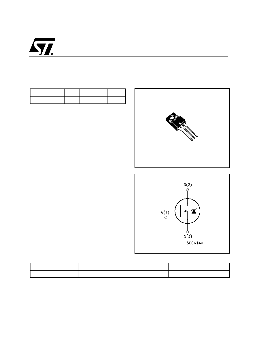
Figure 1: Package
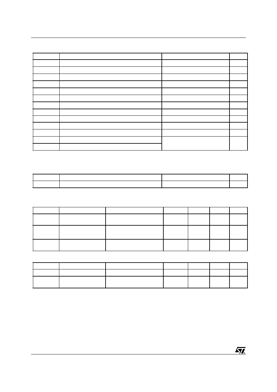
Figure 2: Internal Schematic Diagram
TYPE
V
DSS
R
DS(on)
I
D
STF40NF06
60 V
< 0.028
23 A
TO-220FP
1
2
3
Part Number
Marking
Package
Packaging
STF40NF06
F40NF06
TO-220FP
TUBE
Rev.2
STF40NF06
2/9
Table 3: Absolute Maximum ratings
(1) I
SD
40A, di/dt
300A/µs, V
DD
V
(BR)DSS
, T
j
T
JMAX.
.
(2) Starting T
j
=25∞C, I
D
=20A, V
DD
=30V
( ) Pulse width limited by safe operating area
Table 4: Thermal Data
ELECTRICAL CHARACTERISTICS (T
CASE
=25∞C UNLESS OTHERWISE SPECIFIED)
Table 5: Off
Table 6: On
Symbol
Parameter
Value
Unit
V
DS
Drain-source Voltage (V
GS
= 0)
60
V
V
DGR
Drain-gate Voltage (R
GS
= 20 k
)
60
V
V
GS
Gate- source Voltage
± 20
V
I
D
Drain Current (continuous) at T
C
= 25∞C
23
A
I
D
Drain Current (continuous) at T
C
= 100∞C
16
A
I
DM
( )
Drain Current (pulsed)
92
A
P
TOT
Total Dissipation at T
C
= 25∞C
30
W
Derating Factor
0.2
W/∞C
dv/dt (1)
Peak Diode Recovery voltage slope
10
V/ns
E
AS
(2)
Single Pulse Avalanche Energy
250
mJ
V
ISO
Insulation Withstand Voltage (DC)
2500
V
T
stg
Storage Temperature
≠55 to 175
∞C
T
j
Operating Junction Temperature
Rthj-case
Thermal Resistance Junction-case Max
5.0
∞C/W
T
l
Maximum Lead Temperature For Soldering Purpose
275
∞C
Symbol
Parameter
Test Conditions
Min.
Typ.
Max.
Unit
V
(BR)DSS
Drain-source
Breakdown Voltage
I
D
= 250 µA, V
GS
= 0
60
V
I
DSS
Zero Gate Voltage
Drain Current (V
GS
= 0)
V
DS
= Max Rating
1
µA
V
DS
= Max Rating, T
C
= 125∞C
10
µA
I
GSS
Gate-body Leakage
Current (V
DS
= 0)
V
GS
= ± 20V
±100
nA
Symbol
Parameter
Test Conditions
Min.
Typ.
Max.
Unit
V
GS(th)
Gate Threshold Voltage V
DS
= V
GS
, I
D
= 250µA
2
4
V
R
DS(on)
Static Drain-source On
Resistance
V
GS
= 10V, I
D
= 11.5 A
0.024
0.028
3/9
STF40NF06
ELECTRICAL CHARACTERISTICS (CONTINUED)
Table 7: Dynamic
Table 8: Switching On
Table 9: Switching Off
Table 10: Source Drain Diode
(1) Pulsed: Pulse duration = 300 µs, duty cycle 1.5 %.
(2) Pulse width limited by safe operating area.
Symbol
Parameter
Test Conditions
Min.
Typ.
Max.
Unit
g
fs
(1)
Forward Transconductance
V
DS
= 30 V
I
D
=11.5A
12
S
C
iss
C
oss
C
rss
Input Capacitance
Output Capacitance
Reverse Transfer
Capacitance
V
DS
= 25V, f = 1 MHz, V
GS
= 0
920
225
80
pF
pF
pF
Symbol
Parameter
Test Conditions
Min.
Typ.
Max.
Unit
t
d(on)
t
r
Turn-on Delay Time
Rise Time
V
DD
= 30V, I
D
= 20A
R
G
= 4.7
V
GS
= 10V
(see Figure 16)
27
11
ns
ns
Q
g
Q
gs
Q
gd
Total Gate Charge
Gate-Source Charge
Gate-Drain Charge
V
DD
= 48V, I
D
= 10A,
V
GS
= 10V
32
6.5
15
43
nC
nC
nC
Symbol
Parameter
Test Conditions
Min.
Typ.
Max.
Unit
t
d(off)
t
f
Turn-off-Delay Time
Fall Time
V
DD
= 30V, I
D
= 20A,
R
G
=4.7
,
V
GS
= 10V
(see Figure 16)
27
11
ns
ns
Symbol
Parameter
Test Conditions
Min.
Typ.
Max.
Unit
I
SD
Source-drain Current
23
A
I
SDM
(2)
Source-drain Current (pulsed)
92
A
V
SD
(1)
Forward On Voltage
I
SD
= 23A, V
GS
= 0
1.3
V
t
rr
Q
rr
I
RRM
Reverse Recovery Time
Reverse Recovery Charge
Reverse Recovery Current
I
SD
= 40A, di/dt = 100A/µs,
V
DD
= 10V, T
j
= 150∞C
(see test circuit, Figure 5)
63
150
4.8
ns
nC
A
STF40NF06
4/9
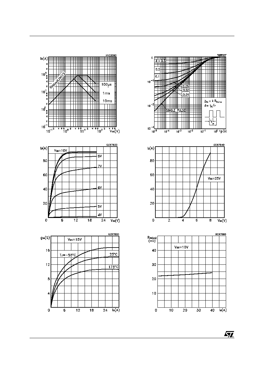
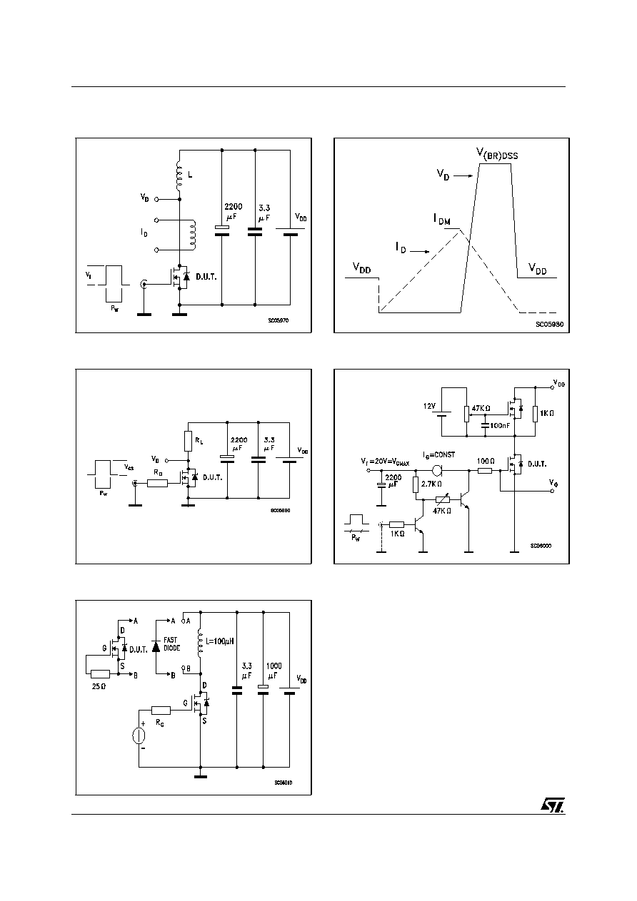
Figure 3: Safe Operating Area
Figure 4: Output Characteristics
Figure 5: Transconductance
Figure 6: Thermal Impedance
Figure 7: Transfer Characteristics
Figure 8: Static Drain-source On Resistance
5/9
STF40NF06
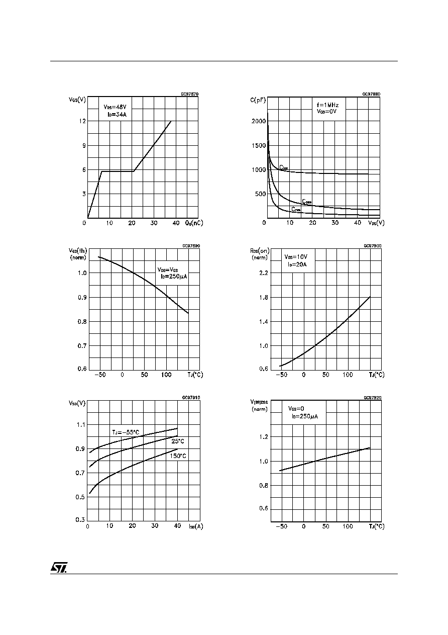
Figure 9: Gate Charge vs Gate-source Voltage
Figure 10: Normalized Gate Thereshold Volt-
age vs Temperature
Figure 11: Source-Drain Diode Forward Char-
acteristics
Figure 12: Capacitance Variations
Figure 13: Normalized On Resistance vs Tem-
perature
Figure 14: Normalized Breakdown Voltage vs
Temperature
STF40NF06
6/9
Figure 15: Unclamped Inductive Load Test Cir-
cuit
Figure 16: Switching Times Test Circuit For
Resistive Load
Figure 17: Test Circuit For Inductive Load
Switching and Diode Recovery Times
Figure 18: Unclamped Inductive Wafeform
Figure 19: Gate Charge Test Circuit
7/9
STF40NF06
L2
A
B
D
E
H
G
L6
F
L3
G1
1 2 3
F2
F1
L7
L4
L5
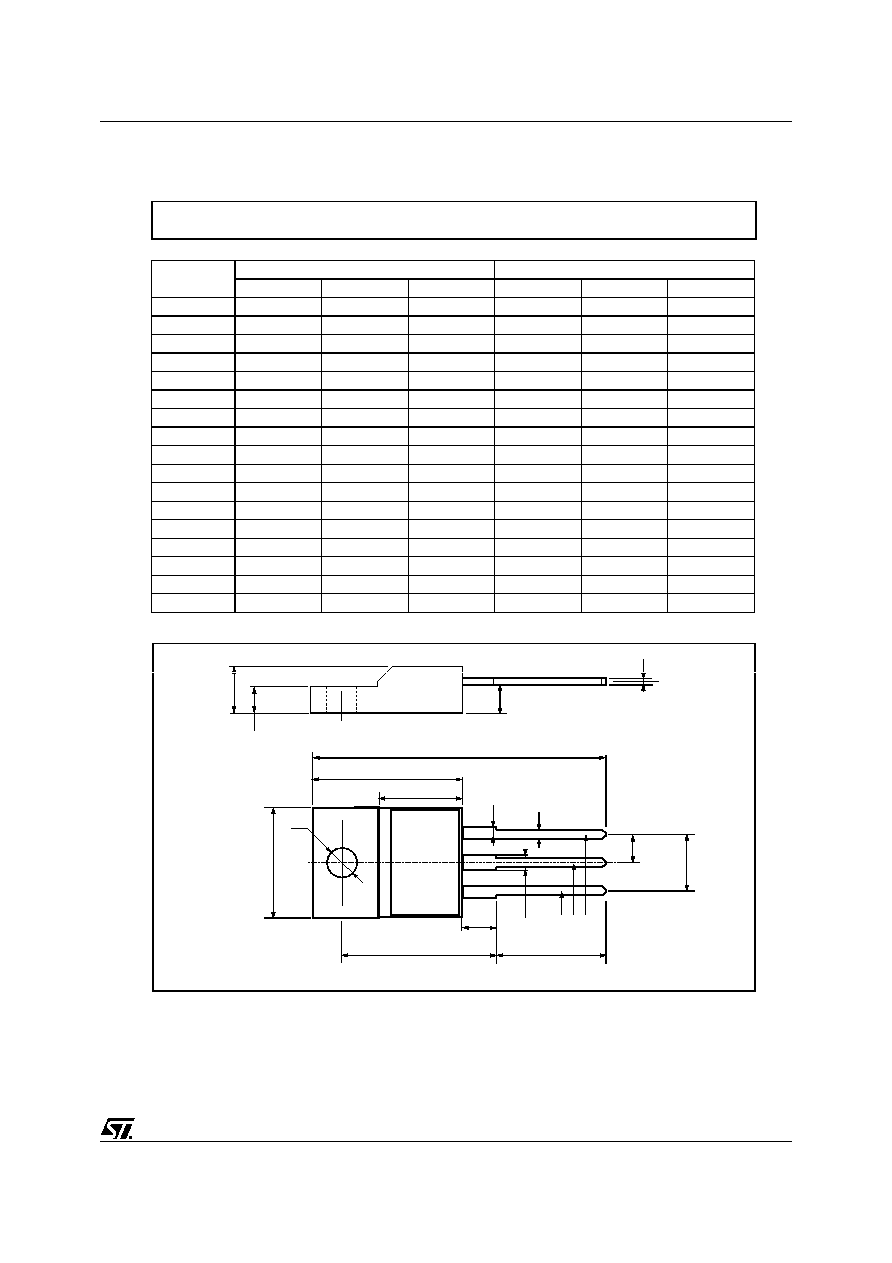
DIM.
mm.
inch
MIN.
TYP
MAX.
MIN.
TYP.
MAX.
A
4.4
4.6
0.173
0.181
B
2.5
2.7
0.098
0.106
D
2.5
2.75
0.098
0.108
E
0.45
0.7
0.017
0.027
F
0.75
1
0.030
0.039
F1
1.15
1.7
0.045
0.067
F2
1.15
1.7
0.045
0.067
G
4.95
5.2
0.195
0.204
G1
2.4
2.7
0.094
0.106
H
10
10.4
0.393
0.409
L2
16
0.630
L3
28.6
30.6
1.126
1.204
L4
9.8
10.6
.0385
0.417
L5
2.9
3.6
0.114
0.141
L6
15.9
16.4
0.626
0.645
L7
9
9.3
0.354
0.366
ÿ
3
3.2
0.118
0.126
TO-220FP MECHANICAL DATA
STF40NF06
8/9
Table 11: Revision History
Date
Revision
Description of Changes
07-Oct-2004
1
First release
11-Nov-2004
2
Final datasheet

9/9
STF40NF06
Information furnished is believed to be accurate and reliable. However, STMicroelectronics assumes no responsibility for the consequences
of use of such information nor for any infringement of patents or other rights of third parties which may result from its use. No license is granted
by implication or otherwise under any patent or patent rights of STMicroelectronics. Specifications mentioned in this publication are subject
to change without notice. This publication supersedes and replaces all information previously supplied. STMicroelectronics products are not
authorized for use as critical components in life support devices or systems without express written approval of STMicroelectronics.
The ST logo is a registered trademark of STMicroelectronics
All other names are the property of their respective owners
© 2004 STMicroelectronics - All Rights Reserved
STMicroelectronics group of companies
Australia - Belgium - Brazil - Canada - China - Czech Republic - Finland - France - Germany - Hong Kong - India - Israel - Italy - Japan -
Malaysia - Malta - Morocco - Singapore - Spain - Sweden - Switzerland - United Kingdom - United States of America
www.st.com