1/6
PRELIMINARY DATA
August 2001
STL35NF10
N-CHANNEL 100V - 0.025
- 35A PowerFLATTM
LOW GATE CHARGE STripFETTM MOSFET
s
TYPICAL R
DS
(on) = 0.025
s
IMPROVED DIE-TO-FOOTPRINT RATIO
s
VERY LOW PROFILE PACKAGE
DESCRIPTION
This Power MOSFET is the second generation of
STMicroelectronics unique "STripFETTM" technolo-
gy. The resulting transistor shows extremely low on-
resistance and minimal gate charge. The new Pow-
erFLATTM package allows a significant reduction in
board space without compromising performance.
APPLICATIONS
s
HIGH EFFICIENCY ISOLATED DC/DC
CONVETERS
ABSOLUTE MAXIMUM RATINGS
(
q
) Pulse width limited by safe operating area
TYPE
V
DSS
R
DS(on)
I
D
STL35NF10
100 V
< 0.030
35 A
Symbol
Parameter
Value
Unit
V
DS
Drain-source Voltage (V
GS
= 0)
100
V
V
DGR
Drain-gate Voltage (R
GS
= 20 k
)
100
V
V
GS
Gate- source Voltage
� 20
V
I
D
Drain Current (continuos) at T
C
= 25�C
Drain Current (continuos) at T
C
= 100�C
35
22
A
A
I
DM
(
q
)
Drain Current (pulsed)
140
A
P
TOT
Total Dissipation at T
C
= 25�C
80
W
Derating Factor
0.64
W/�C
E
AS
(1)
Single Pulse Avalanche Energy
135
mJ
T
stg
Storage Temperature
�65 to 150
�C
T
j
Max. Operating Junction Temperature
�55 to 150
�C
(1) Starting T
j
= 25�C, I
D
= 35A, V
DD
= 50V
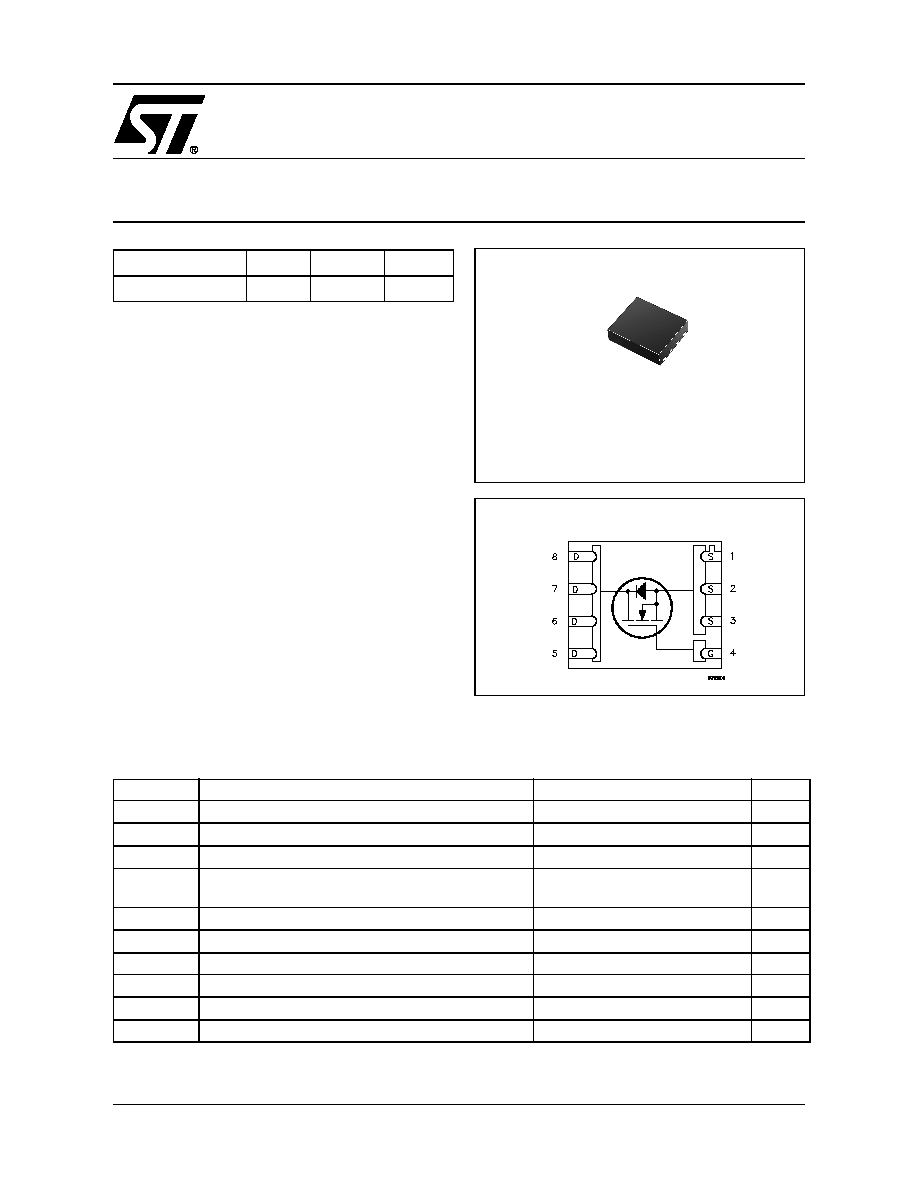
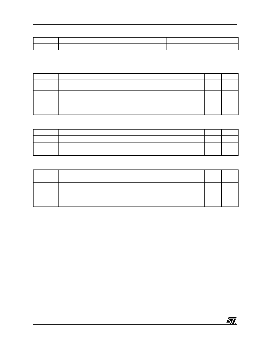
PowerFLATTM(6x5)
(Chip Scale Package)
INTERNAL SCHEMATIC DIAGRAM
STL35NF10
2/6
THERMAL DATA
ELECTRICAL CHARACTERISTICS (TCASE = 25 �C UNLESS OTHERWISE SPECIFIED)
OFF
ON
(1)
DYNAMIC
Rthj-case
Thermal Resistance Junction-case Max
1.56
�C/W
Rthj-amb
Thermal Resistance Junction-ambient Max
50
�C/W
Symbol
Parameter
Test Conditions
Min.
Typ.
Max.
Unit
V
(BR)DSS
Drain-source
Breakdown Voltage
I
D
= 250 �A, V
GS
= 0
100
V
I
DSS
Zero Gate Voltage
Drain Current (V
GS
= 0)
V
DS
= Max Rating
1
�A
V
DS
= Max Rating, T
C
= 125 �C
10
�A
I
GSS
Gate-body Leakage
Current (V
DS
= 0)
V
GS
= � 20V
�100
nA
Symbol
Parameter
Test Conditions
Min.
Typ.
Max.
Unit
V
GS(th)
Gate Threshold Voltage
V
DS
= V
GS
, I
D
= 250�A
2
2.8
4
V
R
DS(on)
Static Drain-source On
Resistance
V
GS
= 10 V, I
D
= 17.5 A
0.025
0.030
Symbol
Parameter
Test Conditions
Min.
Typ.
Max.
Unit
g
fs
(1)
Forward Transconductance
V
DS
=20 V
,
I
D
= 15 A
18
S
C
iss
Input Capacitance
V
DS
= 25 V, f = 1 MHz, V
GS
= 0
1780
pF
C
oss
Output Capacitance
265
pF
C
rss
Reverse Transfer
Capacitance
162
pF
3/6
STL35NF10
ELECTRICAL CHARACTERISTICS (CONTINUED)
SWITCHING ON
SWITCHING OFF
SOURCE DRAIN DIODE
Note: 1. Pulsed: Pulse duration = 300 �s, duty cycle 1.5 %.
2. Pulse width limited by safe operating area.
Symbol
Parameter
Test Conditions
Min.
Typ.
Max.
Unit
t
d(on)
Turn-on Delay Time
V
DD
= 50 V, I
D
= 17.5 A
R
G
= 4.7
V
GS
= 10V
(see test circuit, Figure 1)
28
ns
t
r
Rise Time
63
ns
Q
g
Q
gs
Q
gd
Total Gate Charge
Gate-Source Charge
Gate-Drain Charge
V
DD
= 80 V, I
D
= 35 A,
V
GS
= 10 V
(see test circuit, Figure 2)
60
10
23
80
nC
nC
nC
Symbol
Parameter
Test Conditions
Min.
Typ.
Max.
Unit
t
d(off)
t
f
Turn-off-Delay Time
Fall Time
V
DD
= 50 V, I
D
= 17.5 A,
R
G
= 4.7
,
V
GS
= 10 V
(see test circuit, Figure 1)
84
28
ns
ns
Symbol
Parameter
Test Conditions
Min.
Typ.
Max.
Unit
I
SD
Source-drain Current
35
A
I
SDM
(1)
Source-drain Current (pulsed)
140
A
V
SD
(2)
Forward On Voltage
I
SD
= 18 A, V
GS
= 0
1.2
V
t
rr
Q
rr
I
RRM
Reverse Recovery Time
Reverse Recovery Charge
Reverse Recovery Current
I
SD
= 35 A, di/dt = 100A/�s,
V
DD
= 25 V, T
j
= 150�C
(see test circuit, Figure 3)
114
456
8
ns
nC
A
STL35NF10
4/6
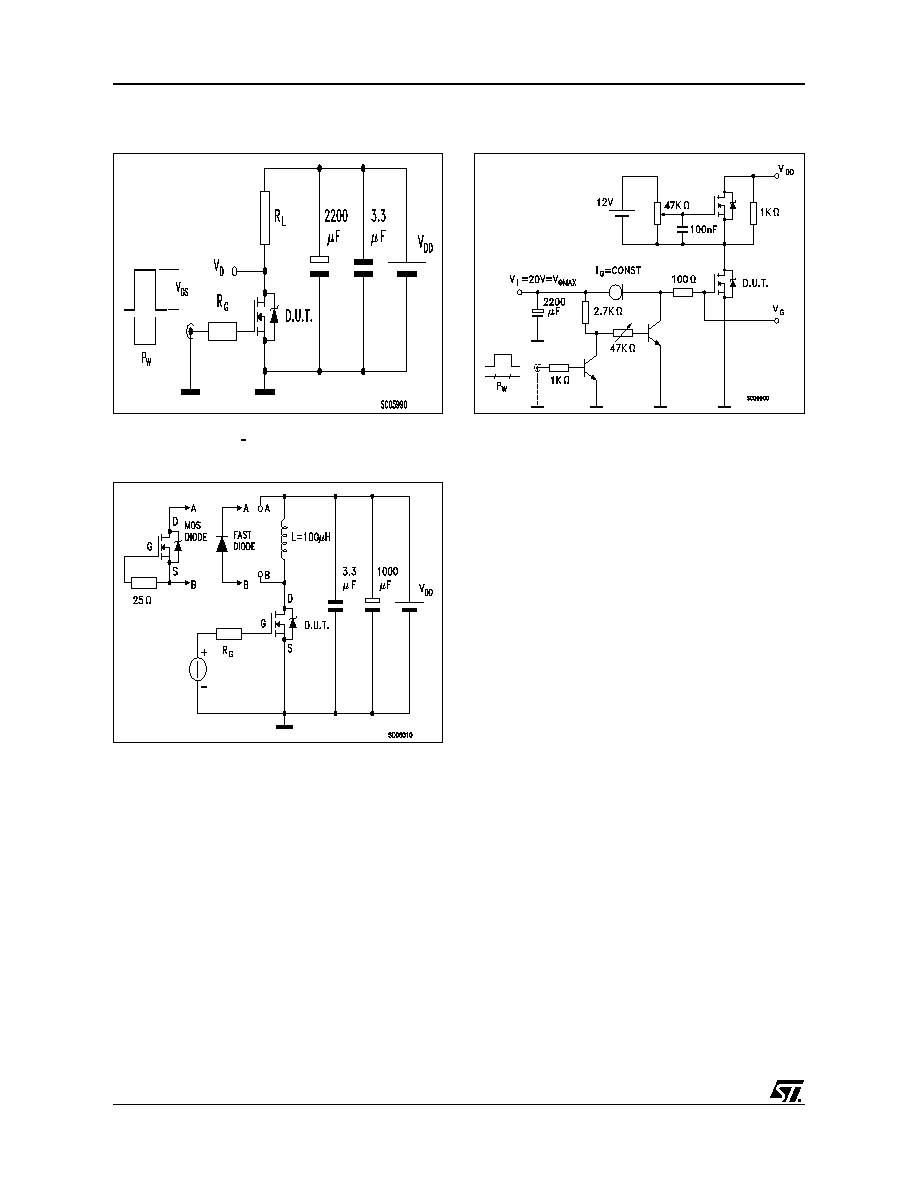
Fig. 3: Test Circuit For Diode Recovery Behaviour
Fig. 2: Gate Charge test Circuit
Fig. 1: Switching Times Test Circuit For
Resistive Load
5/6
STL35NF10
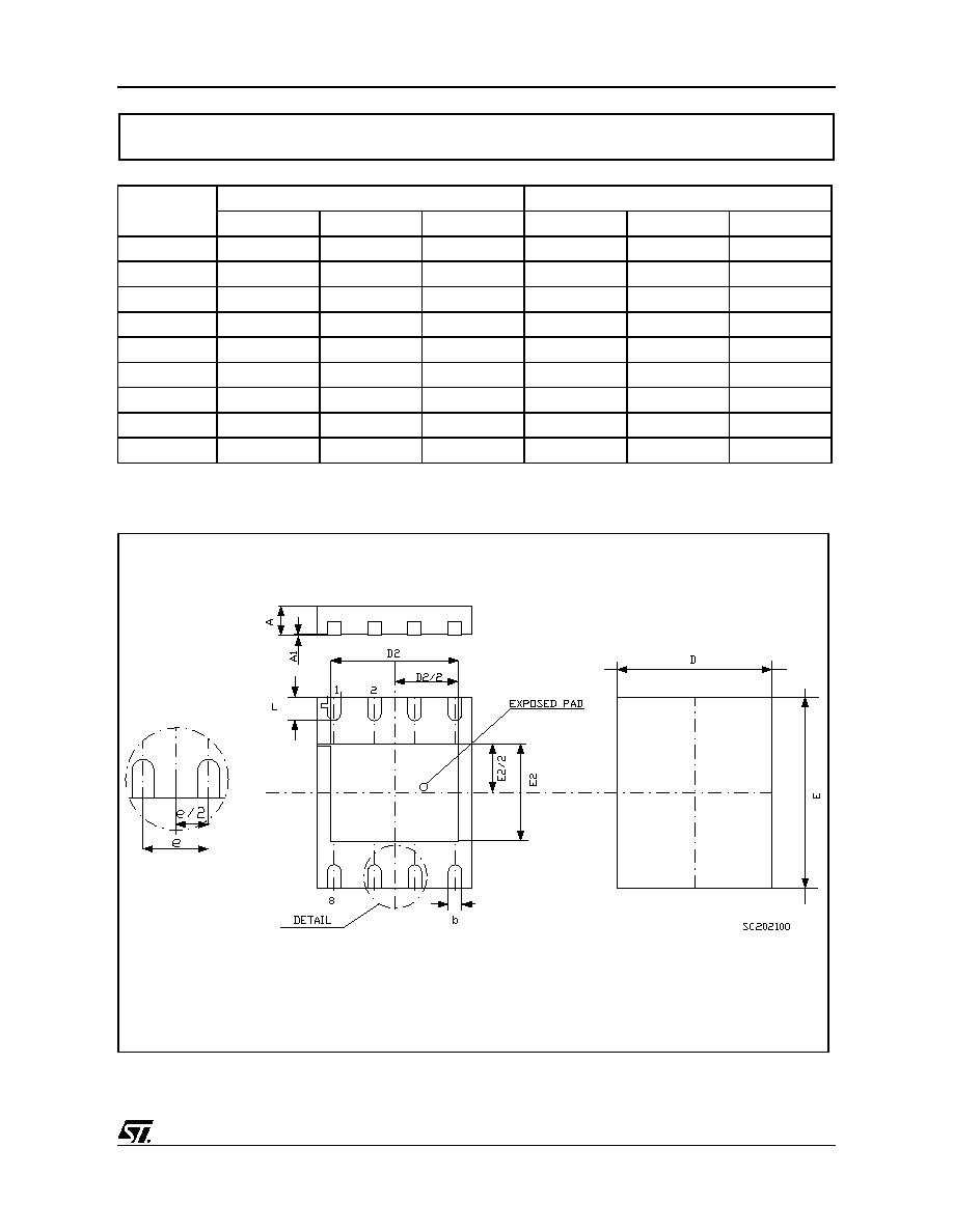
DIM.
mm.
inch
MIN.
TYP
MAX.
MIN.
TYP.
MAX.
A
0.80
1.00
0.031
0.039
A1
0.08
0.003
b
0.36
0.48
0.014
0.018
D
4.89
0.191
D2
3.95
4.05
0.154
0.158
E
6.00
0.235
E2
2.95
3.05
0.115
0.119
e
1.27
0.049
L
0.65
0.85
0.025
0.033
PowerFLATTM(6x5) MECHANICAL DATA