STLC5460
LINE CARD INTERFACE CONTROLLER
BOARD CONTROLLER FOR UP TO 16 ISDN
LINES OR 16 VOICE SUBSCRIBERS.
TWO SERIAL INTERFACES :
-PCM Four bidirectional multiplexes
-GCI One (or two) at 2 Mb/s.
NON BLOCKING SWITCH FOR 128 CHAN-
NELS (16, 32 OR 64 KB/S BANDWIDTH).
N CONSECUTIVE 64 kb/s CHANNELS FROM
AN INPUT MULTIPLEX CAN BE SWITCHED
AS A SINGLE N X 64 kbit/s CHANNEL TO AN
OUTPUT MULTIPLEX AT 2048 kb/s.
TIME SLOT ASSIGNMENT FREELY PRO-
GRAMMABLE FOR EVERY CONNECTED
SUBSCRIBER.
PROGRAMMABLE PCM DATA RATES UP
TO 8192 kb/s.CONSTANT DATA RATE AT 2
Mb/s ON GCI SIDE.
PCM interface :
- Simple and double clock frequency selectable;.
- Programmable clock shift
- Tristate mode control signals for external drivers.
GCI interface :
- Six bits or four bits Command/indicate channel
selectable for analog or digital equipment
- Command/IndicateMonitor channels validated
or not
Microprocessor access to two selected bidirec-
tional channels of GCI and/or PCM.
Multicontrollers for layer 1 functions :
- C/I protocol controller for up to 16 C/I channels
- Monitor protocol controller for up to 16
Monitor channels.
Standard microprocessor interface with multi-
plexed address/data bus or separate address
data buses.
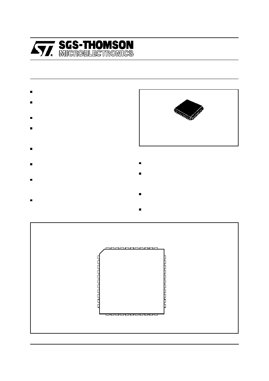
PLCC44 pins PACKAGE
February 1997
1
2
3
5
6
4
7
8
9
10
12
11
13
14
15
16
17
39
38
37
36
34
35
33
32
31
30
29
40
41
42
44 43
23
22
21
19
18
20
28
27
26
24 25
VDD1
A0
RdD3
RxD1
RxD0
RxD2
DOUT1
DOUT0
P0
RES
NRDY/NWAIT
A1
TSC0
TxD0
TSC1
TSC2
TxD1
TxD2
TSC3
TxD3
PFS
PDC
A3
DIN0
DIN1
VSS2
FSC
VDD2
DCL
INT
ALE/AS
NCS
RW/NWR
AD4
AD3
AD2
AD0
A2
AD1
DS/NRD
V
SS
AD7
AD5
AD6
D94TL149B
PIN CONNECTION (Top view)
PLCC44
ORDERING NUMBER: STLC5460
1/54
DESCRIPTION
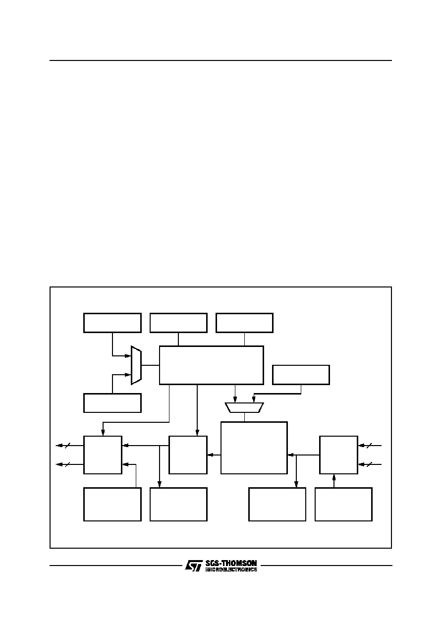
The Line Card Interface Controller, STLC5460, is
a monolithic switching device for the path control
of up to 128 channels of 16, 32, 64 kbps band-
width. Two consecutive 64 kbps channels may
also be handled as a quasi single 128 kbps chan-
nel. For these channels, the LCIC performs non-
blocking space time switching between two serial
interfaces: the system interface (or PCM inter-
face) and the general component interface (GCI).
PCM interface can be programmed to operate at
different data rates between 2048 and 8192 kbps.
The PCM interface consists of up to four duplex
ports with a tristate indication signal for each out-
put line. The GCI interface can be selected to be
PCM interface at 2Mbit/s.
The LCIC can be programmed to communicate
with GCI compatible devices such as STLC3040
(SLIC), STLC5411 (U interface) and others. The
device manages the layer 1 protocol buffering the
Command/Indicate and Monitor channels for GCI
compatible devices.
Due to its capability to switch channels of different
bandwidths, the STLC5460 can handle up to 16
ISDN subscribers with their 2B+D channel struc-
ture in GCI configuration, or up to 16 analog sub-
scribers. Since its interfaces can operate at differ-
ent data rates, the LCIC is an ideal device for
data rate adaptation between PCM interface up to
8Mb/s and GCI at 2Mb/s.
The device gives the possibility of checking the
correct communication inside the PBX or Public
Central Office providing :
- independent PCM delay setting
- PCM comparison function
- Pseudo RandomSequenceGeneratorandAnalyser.
Moreover, the LCIC is one of the key building
blocks for networks with either central, distributed
or mixed signaling and packet data handling ar-
chitectures associated with ST5451 (HDLC con-
troller).
The device is controlled by a standard 8 bit paral-
lel microprocessor interface with a multiplexed
address-data bus. The device may optionally be
controlled by separate address and data buses.
DESTINATION REG
COMMAND REG
SOURCE REGISTER
COMMAND MEMORY
194 WORDS OF 14 BITS
COUNTERS
PARALLEL
SERIAL
SHIFTING
4 PCM
2 GCI
C/I, MON
TRANSMIT
16 INDIPENDENT
CONTROLLERS
SPECIAL
SWITCH AT
16, 32, 64
KB/S
EXTRACTION
2 x 64 Kbit
CHANNEL
(ADDRESS)
(DATA)
(DATA)
SWITCHING
MEMORY
194 BYTES
(4PCM+2GCI + 2
CHANNEL -INSERTION- =
128+64+2=194)
COUNTERS
C/I, MON
RECEIVER
INSERTION
2 x 64 Kbit
CHANNEL
SERIAL
PARALLEL
SHIFTING
4 PCM
2 GCI
1 bit for 16 tristate
6 bits
D94TL160A
BLOCK DIAGRAM
STLC5460
2/54
PIN DEFINITIONS AND FUNCTIONS
Symbol
Pin number
Type (*)
Function
VDD1
1
I
Supply Voltage 5V,
�
5% .
A0
2
I (**)
Non Multiplexed Mode:
this input interfaces to the system's address bus to select an internal
register for a read or write access.
Multiplexed Mode:
A0 at VDD, NRDY/NWAIT pin delivers NWAIT
A0 at VSS, NRDY/NWAIT pin delivers NREADY
RxD3
RxD2
RxD1
RxD0
3
4
5
6
I
Receive PCM interface Data : Serial data is received at these lines at
standard TTL or CMOS levels.
A1
7
I (**)
Non Multiplexed Mode:
this input interfaces to the system's address bus to select an internal
register for a read or write access.
Multiplexed Mode:
A1 at VDD, NCS signal provided by the system is not inverted by the circuit.
A1 at VSS, NCS signal provided by the system is inverted by the circuit.
TSC0
TSC1
TSC2
TSC3
8
10
12
14
OD
Tristate control for the PCM interface. These lines are low when the
corresponding TxD outputs are valid.
TxD0
TxD1
TxD2
TxD3
9
11
13
15
O
Transmit PCM interface Data : Serial data is sent by these lines at standard
TTL or CMOS levels. These pins can be tristated.
PFS
16
I
PCM interface frame synchronization pulse.
PDC
17
I
PCM interface data clock, single or double rate.
A2
18
I (**)
Non Multiplexed Mode:
this input interfaces to the system's address bus to select an intenal register
for a read or write access.
Multiplexed Mode:
A2 at VDD, AS/ALE signal providedby the system is not inverted by the circuit
A2 at VSS, AS/ALE signal provided by the system is inverted by the circuit
AD0
AD1
AD2
AD3
AD4
AD5
AD6
AD7
19
20
21
22
23
24
25
26
I/O
Address Data Bus. If the multiplexed address/data
�
P interface bus mode is
selected these pins transfer data and commands between the
�
P and the
STLC5460.
If a demultiplexed mode is used, these bits interface with the system data
bus.
VSS1
27
I
Ground : 0V
DS/NRD
28
I
Motorola like mode: Data Strobe
Intel Like Mode: Not Read
The signal indicates a read operation, active low
RW/NWR
29
I
Motorola like mode: Read/Write
Intel Like Mode: Not Write
The signal indicates a Write operation, active low.
NCS
30
I
Not Chip select. A low on this line selects the STLC5460 for a read/write
operation.
(*): (I) Input
(O) Output
(IO) In/Output
(OD) Open Drain
(**): With Pull up resistance.
STLC5460
3/54
PIN DEFINITIONS AND FUNCTIONS (continued)
Symbol
Pin n PLCC
Type
Function
AS/ALE
31
I
Multiplexed A/D mode:
used to latch the address from ADn
Non Multiplexed A/D Mode:
This pin at VSS indicates Intel like interfaces
This pin at VDD indicates Motorola like interfaces.
INT
32
OD
Interrupt line, active low.
DCL
33
0
Data clock output.
FSC
34
O
Frame synchronization output.
VDD2
35
I
Power supply : 5V
VSS2
36
I
Ground.
DIN1
37
I
GCI Data input 1
DIN0
38
I
GCI Data input 0
A3
39
I (**)
Non Multiplexed Mode:
this input interfaces to the system's address bus to select an internal
register for a read or write access.
Multiplexed Mode:
A3 at VDD, DS/NRD signal provided by the system is not inverted by the
circuit
A3 at VSS, DS/NRD signal provided by the system isinverted by the circuit
DOUT0
40
O
GCI Data Output 0
DOUT1
41
O
GCI Data Output 1
PO
42
I (**)
P0 at VSS: variable access mode
P0 at VDD: fixed access mode
NRDY/N
WAIT
43
OD
If P0 at VSS:
Intel like mode: this pin delivers NRDY
Motorola mode: this pin delivers NWAIT
RES
44
I
Reset. A logical high on this input forces the STLC5460 into the reset state
(*): (I) Input
(O) Output
(IO) In/Output
(OD) Open Drain
(**): With Pull up resistance.
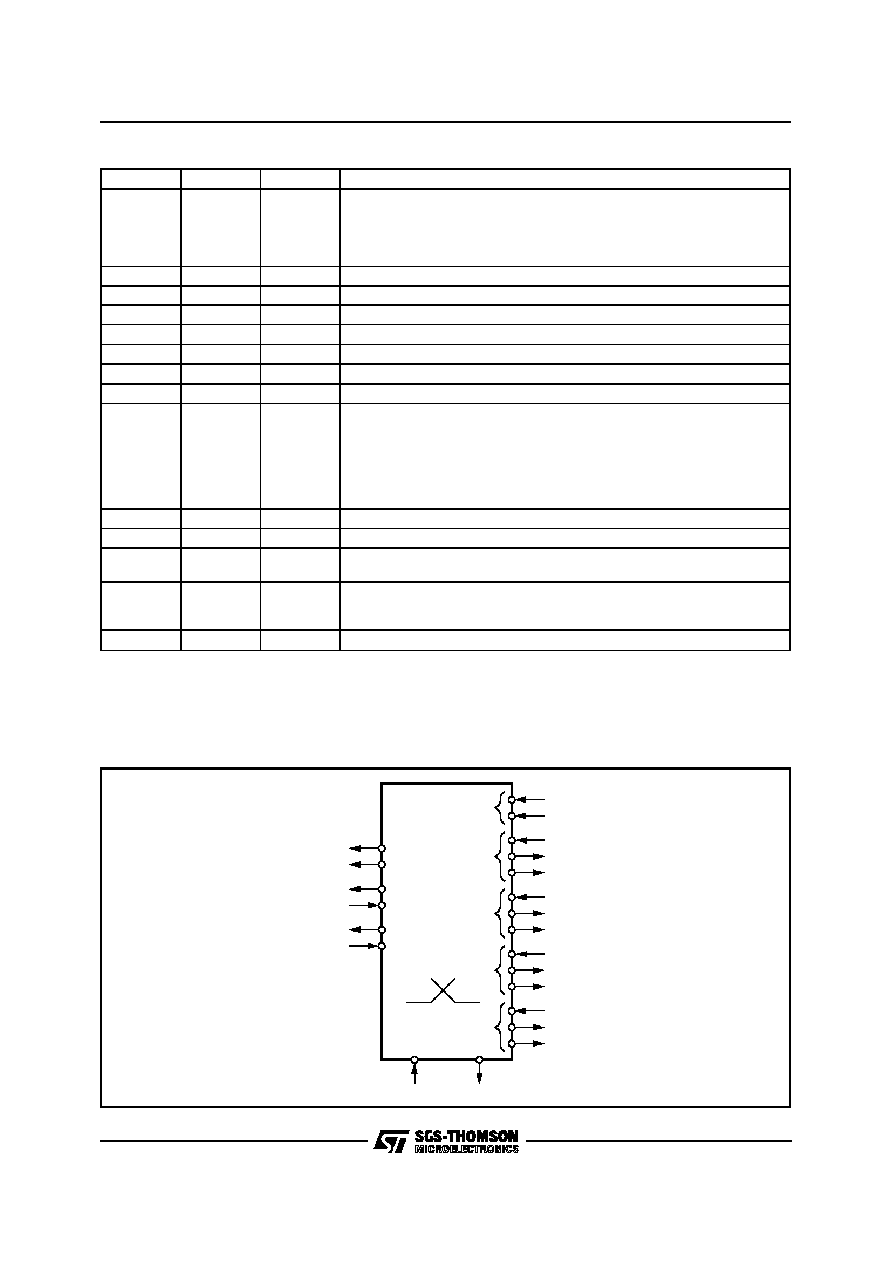
DCL
FSC
DOUT0
DIN0
DOUT1
DIN1
MUX0/GCI0
MUX1/GCI1
LCIC
PCM3
PCM0
PCM1
PCM2
PDC
PFS
RxD3
TxD3
TSC3
RxD0
TxD0
TSC0
RxD1
TxD1
TSC1
RxD2
TxD2
TSC2
MICROPROCESSOR INTERFACE
D94TL159A
CLOCKS
Figure 1: GCI and PCM Interfaces.
STLC5460
4/54
LINE CARD APPLICATIONS
The LCIC is designed to fit both digital and ana-
logue line card architectures.
It supports up to 16 ISDN subscribers or 16 voice
subscribers. The level 1 devices are connected to
ST5451 circuits to perform the D channel han-
dling.
Analogue Line Card
In analogue line cards LCIC controls signalling,
voice and data path of 64 kb/s channels.
When used in combination with L3040/L300 0N, it
allows to implement an optimised line card archi-
tecture:
the LCIC controls the configuration of L3040 and
exchange signalling with the L3040.
Digital Line Card
In digital line cards LCIC controls the configura-
tion of Level 1 circuits (U or S Interface) by
means of MON channel configuration and per-
forms activation/deactivation by means of Com-
mand/Indicate protocol.
LCIC switches the B
channels and can switch the D channels if the
processing is centralised.
FUNCTIONAL DESCRIPTION
PCM INTERFACE
The PCM Interface Registers configure the data
transmitted or received at the PCM port, for one
PCM, the maximum data rate can change de-
pending on the Mode selected:
PCM Mode 0: max rate 2048 kb/s with four PCM
ports active
PCM Mode 1: max rate 4096 kb/s with two PCM
ports active
PCM Mode 2: max rate 8192 kb/s with one PCM
ports active.
The "actual data" rate may be varied in a wide
range without programming.
An automate computes the number of clock per
frame. Hence, the data rate can be stepped in 8,
16 or 32 kb/s in increments in PCM mode 0, 1, 2
respectively.
The clock frequency of PDC is equal to once or
twice the data rate, See fig 1 and 2. When operat-
ing at single rate (2048 kb/s) and not at double
clock frequency (4096 kHz), an onchip clock fre-
quency doubler provides a 4098 kHz clock for the
GCI interface (DCL).
The rising edge of PFS signal is used to deter-
mine the first bit of the first time slot of the frame.
The length of PFS pulse is one bit-time at least
and the length between two pulses can be also
one bit time.
After reset, the LCIC reaches synchronism having
received two consecutive correct PFS pulses.
Synchronisation is considered lost by the device if
the PFS signal is not repeated with the correct
repetition rate which has been stored by the cir-
cuit at the beginning of synchronisation research.
The LSYNC bit in the Interrupt Register indicates
if the component is synchronised or not: a logical
0 indicates the synchronous state, a logical "1"
shows that the synchronism has been lost.
The relation between the framing signal PFS and
the bit stream is controlled by the contents of
IPOF, OPOF and CPOF registers. These regis-
ters denote the number of bit times the PCM
frame is shifted. Each PCM multiplex can be pro-
grammed with different shifts .
Without programming the bit shift function of the
PCM interface, the rising edge of the PFS signal
marks the first bit of input PCM frame and the
first bit of output PCM frame. See Fig 3
GCI Interface
The Monitor and the Command/Indicate channels
may be validated or not, in this second case the
B3 and B4 channels become standard channels
at 64 kb/s.
When validated Command/Indicate channel may
be configured with four bits for digital cards or six
bits for analogue cards.
The clocks (Bit clock and frame clock) are deliv-
ered by the device with double rate clocking or
simple rate clocking.
FSC and DCL are output signals derived from
PFS and PDC which are input signals.
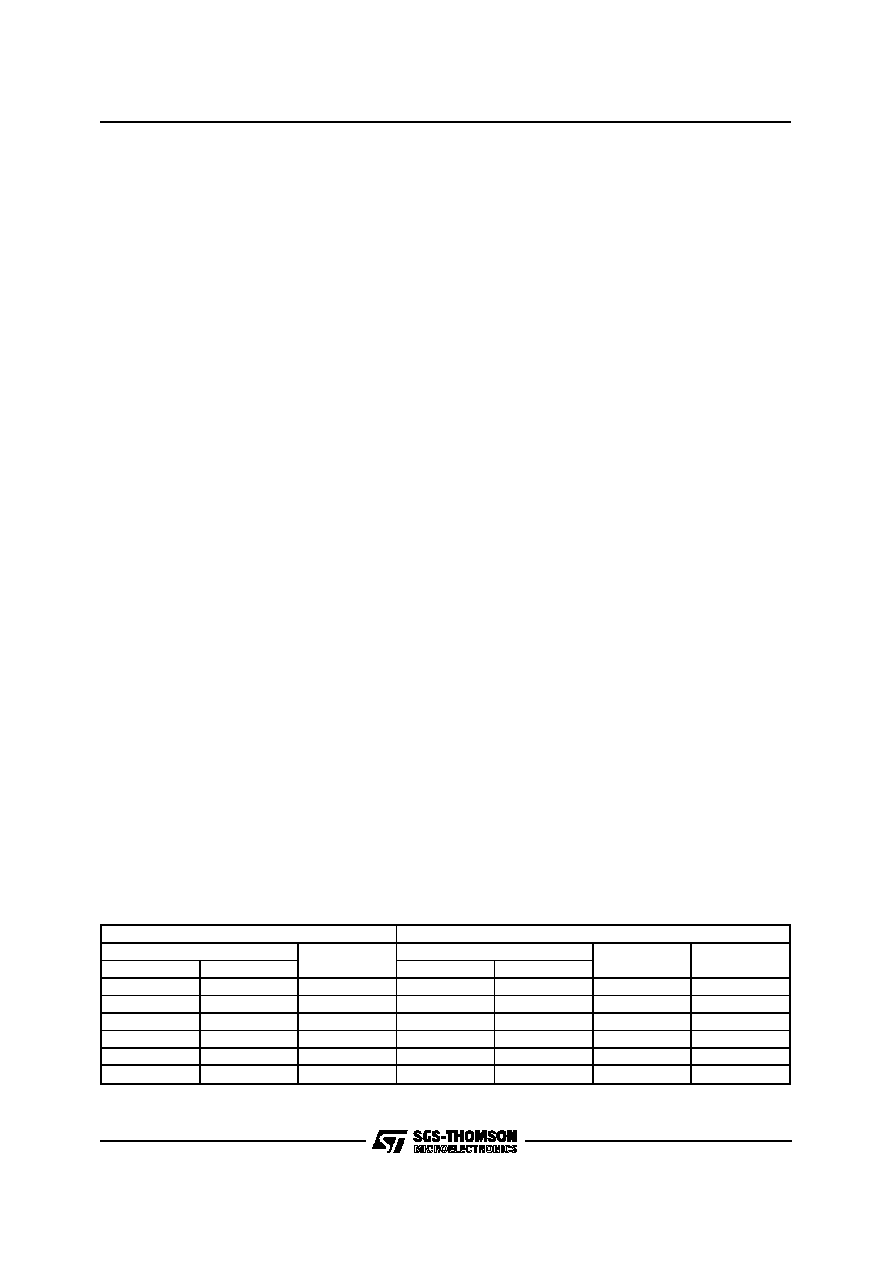
GCI
PCM
DCL clock kHz
Data kb/s
PDC Clock (kHz)
Data rate kb/s
Mode
Simple (*)
Double
Simple
Double
2.048
4.096
2.048
2.048
2.048
Mode 0
2.048
4.096
2.048
4.096
2.048
Mode 0
2.048
4.096
2.048
4.096
4.096
Mode 1
2.048
4.096
2.048
8.192
4.096
Mode 1
2.048
4.096
2.048
8.192
8.192
Mode 2
2.048
4.096
2.048
16.384
8.192
Mode 2
(*) as GCI format but with simple clock.
STLC5460
5/54