1/9
STLC60133N
April 2002
This is preliminary information on a new product now in development. Details are subject to change without notice.
s
LOW NOISE : 4nV/
s
HIGH PEAK OUTPUT CURRENT: 500 mA
s
HIGH SPEED
≠ 140MHz Gain Bandwidth
≠ 30MHz Gain Flatness
≠ 400 V/us Slew Rate
s
LOW POWER OPERATION
≠ ±5V to ±15V Voltage Supply
≠ 3.5 mA/Amp (typ) Supply current
≠ Power reduced Current
s
LOW SINGLE TONE DISTORTION
s
THERMAL AND OVERLOAD PROTECTION
s
HTSSOP28 PACKAGE
s
-40 TO +85∞C OPERATING RANGE
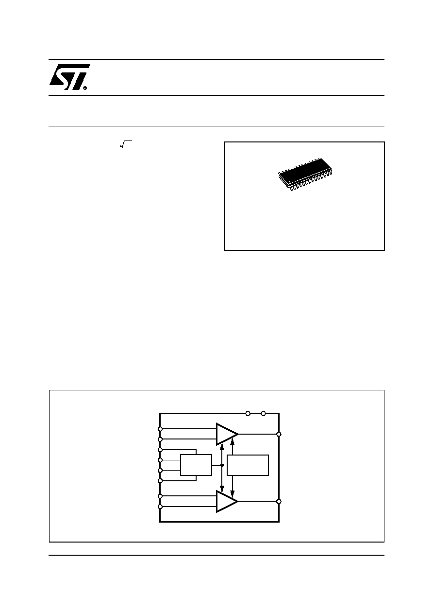
DESCRIPTION
The STLC60133N is a dual amplifier featuring a
high slew rate and a large bandwidth optimized for
XDSL applications. The device is available in a
HTSSOP 28 pin package (4x9 mm) with an exposed
leadframe.
Thanks to its small package this line driver is suitable
for high density ADSL line card.
Two digital pins (PWDN0 and PWDN1) allow the driv-
er to work in full performance mode, in low-power
mode or two intermediate bias states.
The low-power mode biases the output stage in order
to provide a low impedance at the amplifier outputs
for back termination.
The STLC60133N is designed optimizing bandwidth
and distortion performances. For proper device oper-
ating it is necessary to work with a gain level greater
than 15.6dB.
Typical differential gain is normally +27dB, while typ-
ical common mode gain is 15.6dB
H z
HTSSOP28
ORDERING NUMBER: STLC60133N
Temperature Range: -40∞C to +85∞C
PRODUCT PREVIEW
XDSL LINE DRIVER
Figure 1. BLOCK DIAGRAM
TH DETCT.
OUT1
+V
S
-V
S
OUT2
IN1N
IN1P
PWDN0
PWDN1
BIAS
DGND
IN2N
IN2P
Op1
-
+
-
+
Op2
LOGIC
D00TL462A
STLC60133N
2/9
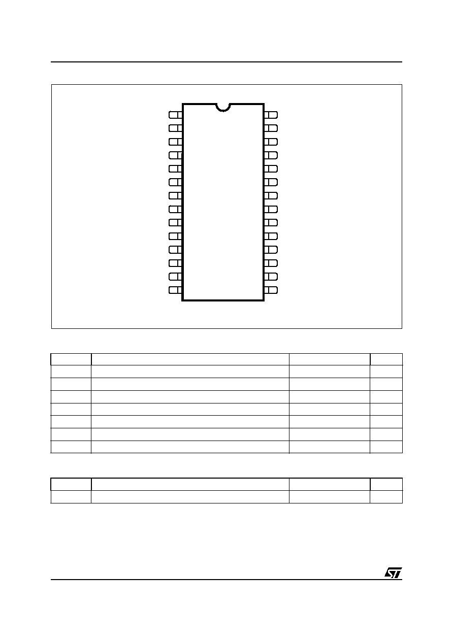
PIN CONNECTION
ABSOLUTE MAXIMUM RATINGS
THERMAL DATA
Symbol
Parameter
Value
Unit
V
CC
Positive Supply voltage (note1)
+16.5
V
V
SS
Negative Supply voltage (note1)
-16.5
V
V
id
Differential Input Voltage (note2)
±5
V
V
i
Common mode Input Voltage
±1
V
T
op
Operating Free Air Temperature Range
-40 to +85
∞C
T
stg
Storage temperature
-65 to +150
∞C
T
j
Junction temperature
165
∞C
Symbol
Parameter
Value
Unit
R
thj-amb
Thermal resistance junction to ambient (note 3)
29
∞C/W
RES
N.C.
N.C.
IN2P
IN2N
+V
S
OUT2
+V
S
OUT1
DGND
-V
S
-V
S
PWDN1
BIAS
N.C.
N.C.
N.C.
RES
1
3
2
4
5
6
7
8
9
26
25
24
23
22
20
21
19
27
10
28
IN1N
N.C.
D00TL463A
IN1P
N.C
N.C.
N.C.
N.C.
PWDN0
11
12
13
18
16
17
15
14
N.C.
N.C.
3/9
STLC60133N
OPERATING RANGE
Notes
1) All voltages values , except differential voltage , are with respect to network ground terminal .
2) Differential voltages are non-inverting input terminal with respect to the inverting input terminal
3) Specification is for device on a 4 layer board within 10 square inches of oz. copper at +85∞C and 200m/s air velocity. With 0m/s air velocity
the parameter increases up to 33∞C/W
.
PIN DESCRIPTION
Power Down Management
The STLC60133N provides several quiescent bias levels from full performance, to reduced bias (in three steps
through PWDN0/1 pins) or to full OFF operation (through BIAS pin). According to the different XDSL application
(both site CO and CPE), different bias levels can be chosen maintaining good MTPR performances. In the fol-
lowing table are shown the bias levels versus the PWDN values.
Symbol
Parameter
Value
Unit
T
op
Operating Temperature Range
-40 to 85
∞C
V
CC
Positive Supply voltage (note1)
+5 to +15
V
V
SS
Negative Supply voltage (note1)
-5 to -15
V
V
DGND
Digital Ground level
V
SS
<V
DGND
<V
CC
-5
V
V
icm
Common Mode Input Voltage Range
±1
V
N∞
Pin
Description
1, 28
RES
To be left not connected
2, 3, 12, 13, 14, 15, 16, 17, 19,
25, 26, 27
NC
Not Connected
4
IN2P
Non Inverting Input of Op. Amplifier 2
5
IN2N
Inverting Input of Op. Amplifier 2
6
OUT2
Ouput of Op. Amplifier 2
7, 8
+Vs
Positive Supply Voltage
9
OUT1
Ouput of Op. Amplifier 1
10
IN1N
Inverting Input of Op. Amplifier 1
11
IN1P
Non Inverting Input of Op. Amplifier 1
18
PWDN0
Power Down 0 logic input
20
DGND
Digital GND
21, 22
-Vs
Negative Supply Voltage
23
BIAS
Bias Control pin
24
PWDN1
Power Down 1 logic input
PWDN1
PWDN0
Bias Level
1
1
100%
1
0
80%
0
1
60%
0
0
40% (low Zout but not OFF)
X
X
Full OFF (High Zout via 75uA pulled out of BIAS pin)
STLC60133N
4/9
The bias level is programmed by the TTL logic level applied to the PWDN pins. The DGND pin is the logic
ground reference for the PWDN pins. For normal operation the BIAS pin shall be left open.
The BIAS control pin can be used to adjust the internal biasing and thus the quiescent current. By pulling out a
current of 0
µ
A to 50
µ
A, the quiescent current can be adjusted from 100% (full ON) to a full OFF condition. How-
ever, considering the internal parameter spread to full shutdown the STLC60133N is recommended to pull down
a 75
µ
A current from the BIAS pin. In the following figure is shown an implementation of a complete amplifier
shutdown. To partially reduce the internal biasing also the PWDN pins can be used.
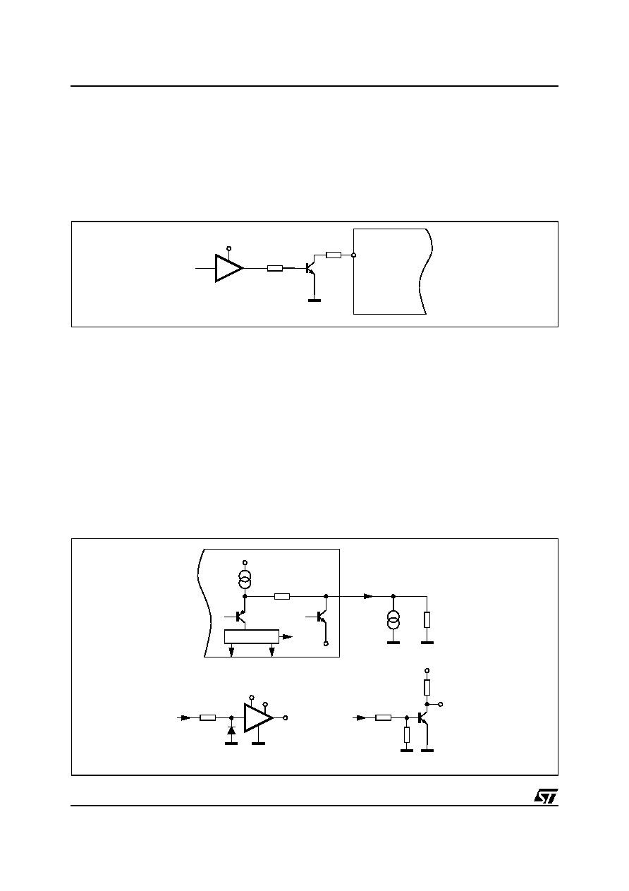
Figure 2. Logic drive of bias pin for complete Amplifier Shutdown.
THERMAL SHUTDOWN
A thermal protection is embedded in the STLC60133N. In case of thermal overload the device is shut down at
160∞C and returns to normal operation when the temperature becomes lower than 145∞C.
During the thermal shutdown the voltage at the BIAS pin goes to the DGND rail; when the device returns to the
normal operation the voltage at the BIAS pin goes to the positive rail. In this condition the BIAS pin can be used
as thermal overload indicator.
MAXIMUM POWER DISSIPATION
Maximum Junction Temperature allowed for proper device operation is T
j
= 140∞C. A Typical Thermal Resis-
tance Junction to ambient of 29∞C/W can be obtained mounting the device on a 4 layer board whithin 10 square
inches of copper and having the exposed pad contacting a proper copper area . It shall be noted that the ex-
posed pad of the device is electrically not connected to the V
SS
negative supply.
Figure 3. Shutdown and alarm circuit
3.3V
BIAS
50K
R1
D01TL519
R1 = 47K
for
±
12V
R1 = 22K
for
±
6V
R2
STLC60133N
V
CC
V
CC
+5V
ALARM
OR
V
EE
BIAS
BIAS
BIAS
BIAS
V
BIAS
=V
CC
-1.5V
OR
0-200
µ
A
10K
PWDN0
PWDN1
1/4 HCF40109B
ST
SHUT
DOWN
50
µ
A
10K
1M
10K
100K
ALARM
D01TL520
MIN
350
+5V
STLC60133N
5/9
STLC60133N
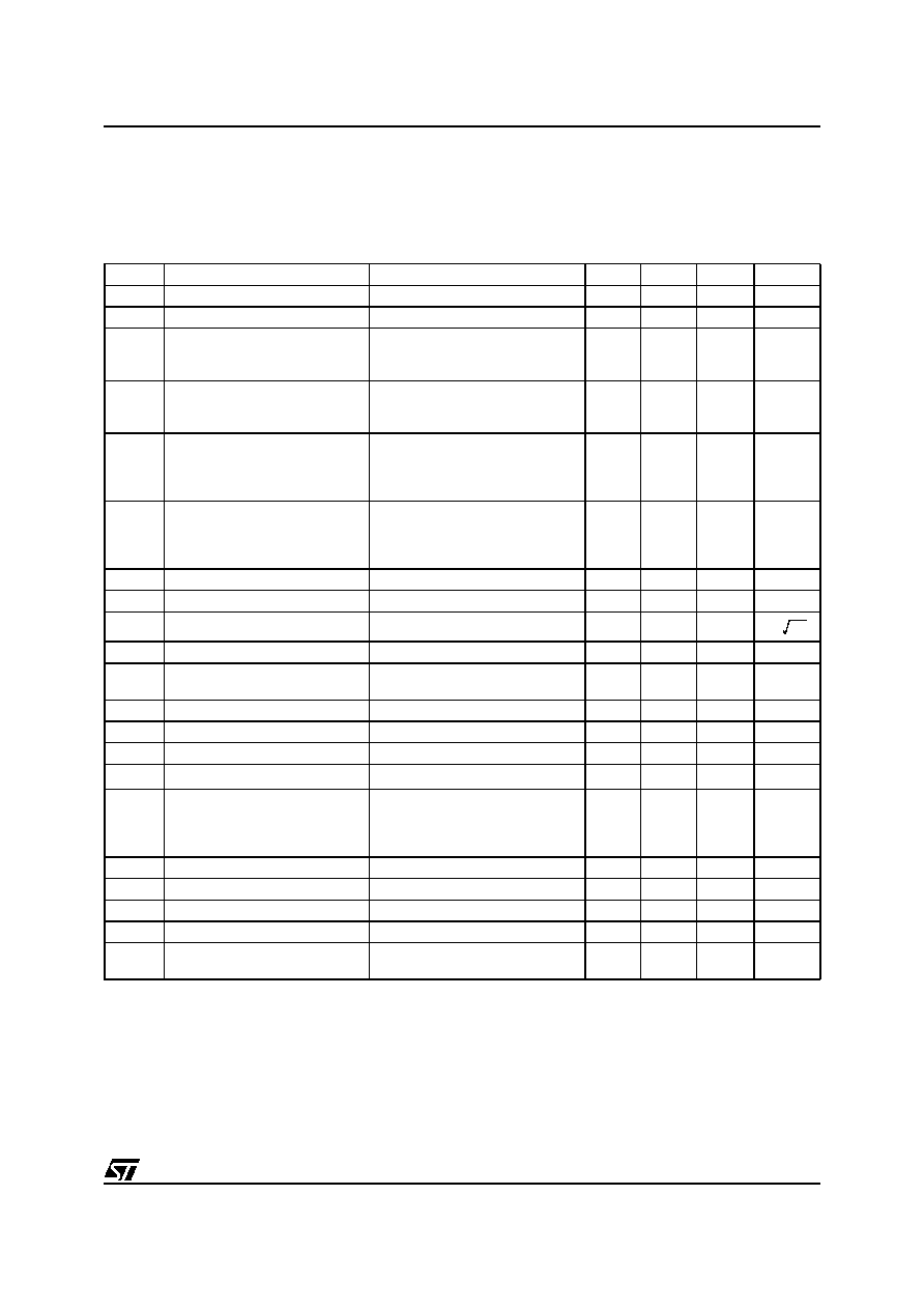
ELECTRICAL CHARACTERISTCS
Test Conditions: (V
CC
= ±12V , Tamb = 0 to 70∞C , Single amplifier in normal condition (PWDN0 = 1, PWDN1 = 1),
unless otherwise specified). The limits listed below are guaranted in the above temperature range (0-70∞C) by
specific testing at different temperature or by product characterisation.
TRANSMISSION PATH
Notes: 1. The output stage of the STLC60133N is designed for maximum load current capability. As a result, shorting the output to common
can cause the STLC60133N to source or sink 1.4A.
2. Guaranteed by product characterization.
Symbol
Parameter
Test Condition
Min.
Typ.
Max.
Unit
SR
Slew Rate
G = 6, Vout = 2Vpp
400
V/us
GBW
Gain Bandwidth
G = 6, Vout = 2Vpp, f = 5MHz
90
140
MHz
THD
Single ended Distortion
G = 6, f = 1MHz, Vout = 12Vpp,
Rl = 16.5
Rl = 100
-47
-52
dBc
DTHD
Differential THD
(2)
G = 6, f = 1MHz, Vout = 24Vpp,
Rl = 33
Rl = 100
-50
-55
dBc
IMD
Single ended IMD
G = 6, Vout = 3Vp each tone,
f = 500KHz,
f = 10KHz
Rl = 16.5
Rl = 100
-70
-75
dBc
DIMD
Differential IMD
(2)
G = 6, Vout = 6Vp each tone,
f = 500KHz,
f = 10KHz
Rl = 33
Rl = 100
-66
-72
dBc
IB
Input Biasing
5
µ
A
OZ
Output Impedance
PWDN0 = PWDN1 = 0; f = 1MHz
2
VN
Voltage Noise (RTI)
f = 30KHz
4
10
nV/
IOV
Input Offset Voltage
6
mV
ICMR
Input Common Mode Voltage
Range
f = 1 MHz
-1
+1
V
CMRR
Common Mode Rejection Ratio
f = 1 MHz, Vin = 100mV
40
dB
OVS
Output Voltage Swing
Single ended, Rl = 100
, G = 6
-11
+11
V
LOC
Linear Output Current
Single ended, Rl = 10
, G = 6
400
600
mA
SCC
Short Circuit Current
(1)
Single ended
1000
1400
mA
QC
Quiescent Current
PWDN1, PWDN0 = 1,1
PWDN1, PWDN0 = 1,0
PWDN1, PWDN0 = 0,1
PWDN1, PWDN0 = 0,0
3.5
2.9
2.2
1.6
mA/Amp
SC
Shutdown Current
75
µ
A out of Bias pin
1.5
2.0
mA/Amp
PSRR
Power Supply Rejection ratio
f = 500kHz, V = 100mV
30
dB
BIASV
Bias Pin Voltage
10
10.5
V
DCG
DC Gain
80
dB
HIZ
Output impedance in Shut Down
mode
500
k
Hz