STP80NS04Z
N - CHANNEL CLAMPED 7.5m
- 80A - TO-220
FULLY PROTECTED MESH OVERLAY
TM
MOSFET
s
TYPICAL R
DS(on)
= 0.0075
s
100% AVALANCHE TESTED
s
LOW CAPACITANCE AND GATE CHARGE
s
175
o
C MAXIMUM JUNCTION
TEMPERATURE
DESCRIPTION
This fully clamped Mosfet is produced by using
the latest advanced Company's Mesh Overlay
process which is based on a novel strip layout.
The inherent benefits of the new technology
coupled with the extra clamping capabilities make
this product particularly suitable for the harshest
operation conditions such as those encountered
in
the
automotive environment.
Any
other
application requiring extra ruggedness is also
recommended.
APPLICATIONS
s
ABS, SOLENOID DRIVERS
s
MOTOR CONTROL
s
DC-DC CONVERTERS
Æ
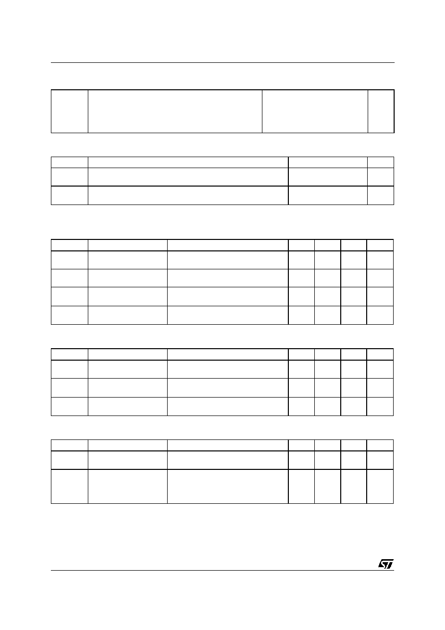
INTERNAL SCHEMATIC DIAGRAM
December 1999
1
2
3
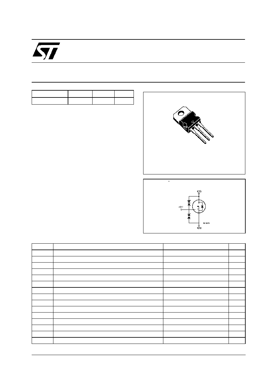
TO-220
ABSOLUTE MAXIMUM RATINGS
Symbol
Parameter
Value
Un it
V
DS
Drain-source Voltage (V
GS
= 0)
CLAMPED
V
V
DG
Drain- gate Voltage
CLAMPED
V
V
GS
G ate-source Volt age
CLAMPED
V
I
D
Drain Current (continuous) at T
c
= 25
o
C
80
A
I
D
Drain Current (continuous) at T
c
= 100
o
C
60
A
I
DG
Drain Gate Current (continuous)
±
50
mA
I
G S
G ate Source Current (cont inuous)
±
50
mA
I
DM
(
∑
)
Drain Current (pulsed)
320
A
P
tot
T otal Dissipation at T
c
= 25
o
C
160
W
Derating Factor
1.06
W /
o
C
V
ESD
(G-S )
G ate-Source ESD (HBM - C= 100pF , R=1.5 k
)
2
kV
V
ESD
(G -D)
G ate-Drain ESD (HBM - C= 100pF, R=1.5 k
)
4
kV
V
ESD
( D-S)
Drain-Source ESD (HBM - C= 100pF, R=1.5 k
)
4
kV
T
s tg
Storage Temperature
-65 to 175
o
C
T
j
Max. Operating Junction Temperature
-40 to 175
o
C
(
∑
) Pulse width limited by safe operating area
(
1
) I
SD
80 A, di/dt
300 A/
µ
s, V
DD
V
(BR)DSS
, T
j
T
JMAX
TYPE
V
DSS
R
DS(on)
I
D
STP80NS04Z
CLAMPED
<0.008
80 A
1/8
THERMAL DATA
R
thj -case
R
thj -case
R
thj -amb
R
thc-sink
T
l
Thermal Resistance Junction-case
Max
Thermal Resistance Junction-case
Typ
Thermal Resistance Junction-ambient
Max
Thermal Resistance Case-sink
Typ
Maximum Lead Temperature F or Soldering Purpose
0.94
0.65
62.5
0.5
300
o
C/W
o
C/W
o
C/W
o
C/W
o
C
AVALANCHE CHARACTERISTICS
Symbo l
Parameter
Max Value
Unit
I
AR
Avalanche Current, Repetitive or Not-Repetitive
(pulse width limited by T
j
max,
< 1%)
80
A
E
AS
Single Pulse Avalanche Energy
(starting T
j
= 25
o
C, I
D
= I
AR
, V
DD
= 30 V)
500
mJ
ELECTRICAL CHARACTERISTICS (T
case
= 25
o
C unless otherwise specified)
OFF
Symbo l
Parameter
Test Con ditions
Min.
Typ.
Max.
Unit
V
CLAMP
Drain-Gate Breakdown
Voltage
I
D
= 1 mA
V
GS
= 0
-40 < T
j
< 175
o
C
33
V
I
DSS
Zero Gat e Voltage
Drain Current (V
GS
= 0)
V
DS
= 16 V
T
j
= 175
o
C
50
µ
A
I
G SS
Gat e-body Leakage
Current (V
DS
= 0)
V
GS
=
±
10 V
T
j
= 175
o
C
V
GS
=
±
16 V
T
j
= 175
o
C
50
150
µ
A
µ
A
V
GSS
Gat e-Source
Breakdown Voltage
I
G
= 100
µ
A
18
V
ON (
)
Symbo l
Parameter
Test Con ditions
Min.
Typ.
Max.
Unit
V
G S(th)
Gat e Threshold Voltage V
DS
=V
GS
I
D
= 1 mA
-40 < T
j
< 150
o
C
1. 7
3
4. 2
V
R
DS(on)
Static Drain-source On
Resistance
V
GS
= 10V
I
D
= 40 A
V
GS
= 16V
I
D
= 40 A
8
7.5
9
8
m
m
I
D(o n)
On State Drain Current
V
DS
> I
D(o n)
x R
DS(on )ma x
V
GS
= 10 V
80
A
DYNAMIC
Symbo l
Parameter
Test Con ditions
Min.
Typ.
Max.
Unit
g
f s
(
)
Forward
Transconductance
V
DS
> I
D(o n)
x R
DS(on )ma x
I
D
=40 A
30
50
S
C
iss
C
os s
C
rss
Input Capacitance
Out put Capacitance
Reverse Transfer
Capacitance
V
DS
= 25 V
f = 1 MHz
V
GS
= 0
4000
1250
230
5400
1700
320
pF
pF
pF
STP80NS04Z
2/8
ELECTRICAL CHARACTERISTICS (continued)
SWITCHING ON
Symbo l
Parameter
Test Con ditions
Min.
Typ.
Max.
Unit
Q
g
Q
gs
Q
gd
Tot al G ate Charge
Gat e-Source Charge
Gat e-Drain Charge
V
DD
= 16 V
I
D
= 80 A
V
G S
= 10 V
105
24
41
142
nC
nC
nC
SWITCHING OFF
Symbo l
Parameter
Test Con ditions
Min.
Typ.
Max.
Unit
t
r (Voff)
t
f
t
c
Off -volt age Rise T ime
Fall T ime
Cross-over Time
V
CLAM P
= 30 V
I
D
= 80 A
R
G
=4.7
V
GS
= 10 V
(see t est circuit, f igure 5)
60
140
220
80
190
300
ns
ns
ns
SOURCE DRAIN DIODE
Symbo l
Parameter
Test Con ditions
Min.
Typ.
Max.
Unit
I
SD
I
SDM
(
∑
)
Source-drain Current
Source-drain Current
(pulsed)
80
320
A
A
V
SD
(
)
Forward On Voltage
I
SD
= 80 A
V
GS
= 0
1. 5
V
t
rr
Q
rr
I
RRM
Reverse Recovery
Time
Reverse Recovery
Charge
Reverse Recovery
Current
I
SD
= 80 A
di/ dt = 100 A/
µ
s
V
r
= 25 V
T
j
= 150
o
C
(see t est circuit, f igure 5)
75
0.21
6
ns
µ
C
A
(
) Pulsed: Pulse duration = 300
µ
s, duty cycle 1.5 %
(
∑
) Pulse width limited by safe operating area
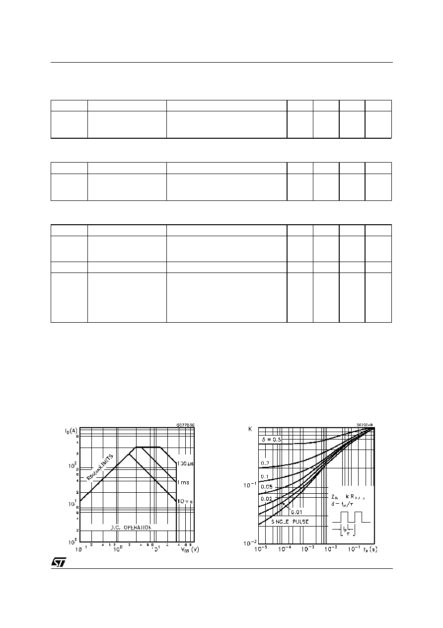
Safe Operating Area
Thermal Impedance
STP80NS04Z
3/8
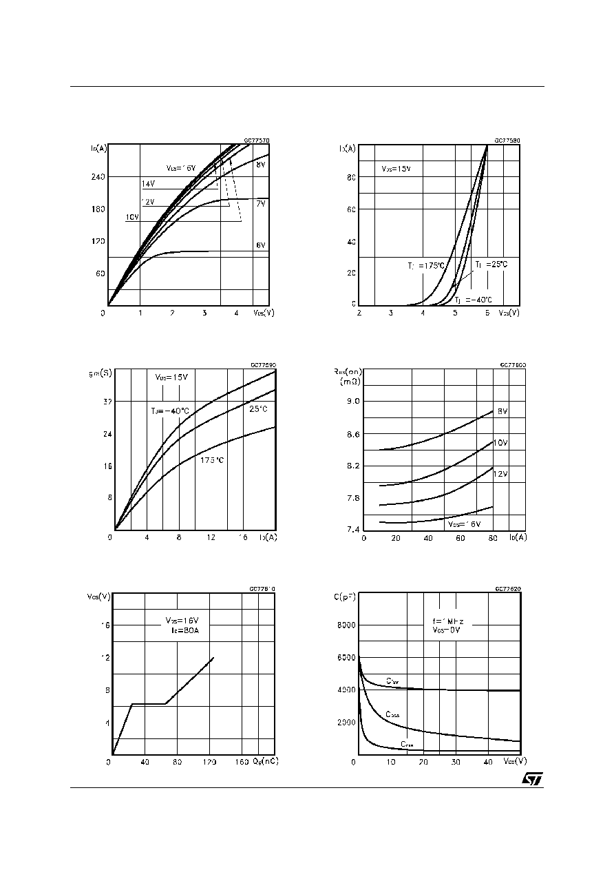
Output Characteristics
Transconductance
Gate Charge vs Gate-source Voltage
Transfer Characteristics
Static Drain-source On Resistance
Capacitance Variations
STP80NS04Z
4/8
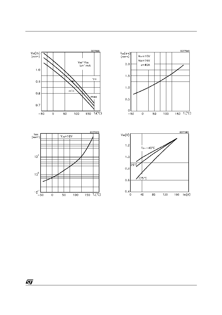
Normalized Gate Threshold Voltage vs
Temperature
Zero Gate Voltage Drain Current vs
Temperature
Normalized On Resistance vs Temperature
Source-drain Diode Forward Characteristics
STP80NS04Z
5/8
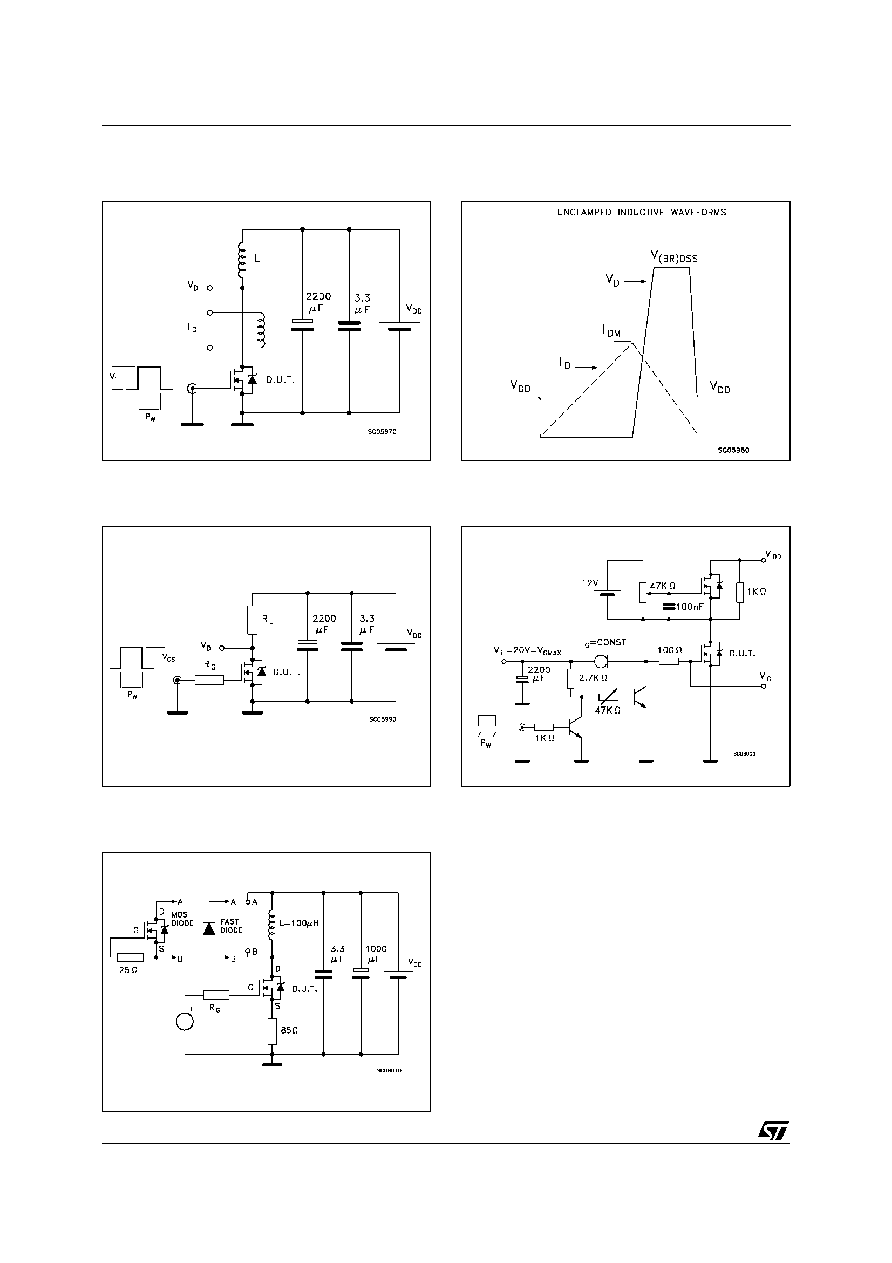
Fig. 1: Unclamped Inductive Load Test Circuit
Fig. 3: Switching Times Test Circuits For
Resistive Load
Fig. 2: Unclamped Inductive Waveform
Fig. 4: Gate Charge test Circuit
Fig. 5: Test Circuit For Inductive Load Switching
And Diode Recovery Times
STP80NS04Z
6/8
DIM.
mm
inch
MIN.
TYP.
MAX.
MIN.
TYP.
MAX.
A
4.40
4.60
0.173
0.181
C
1.23
1.32
0.048
0.051
D
2.40
2.72
0.094
0.107
D1
1.27
0.050
E
0.49
0.70
0.019
0.027
F
0.61
0.88
0.024
0.034
F1
1.14
1.70
0.044
0.067
F2
1.14
1.70
0.044
0.067
G
4.95
5.15
0.194
0.203
G1
2.4
2.7
0.094
0.106
H2
10.0
10.40
0.393
0.409
L2
16.4
0.645
L4
13.0
14.0
0.511
0.551
L5
2.65
2.95
0.104
0.116
L6
15.25
15.75
0.600
0.620
L7
6.2
6.6
0.244
0.260
L9
3.5
3.93
0.137
0.154
DIA.
3.75
3.85
0.147
0.151
L6
A
C
D
E
D1
F
G
L7
L2
Dia.
F1
L5
L4
H2
L9
F2
G1
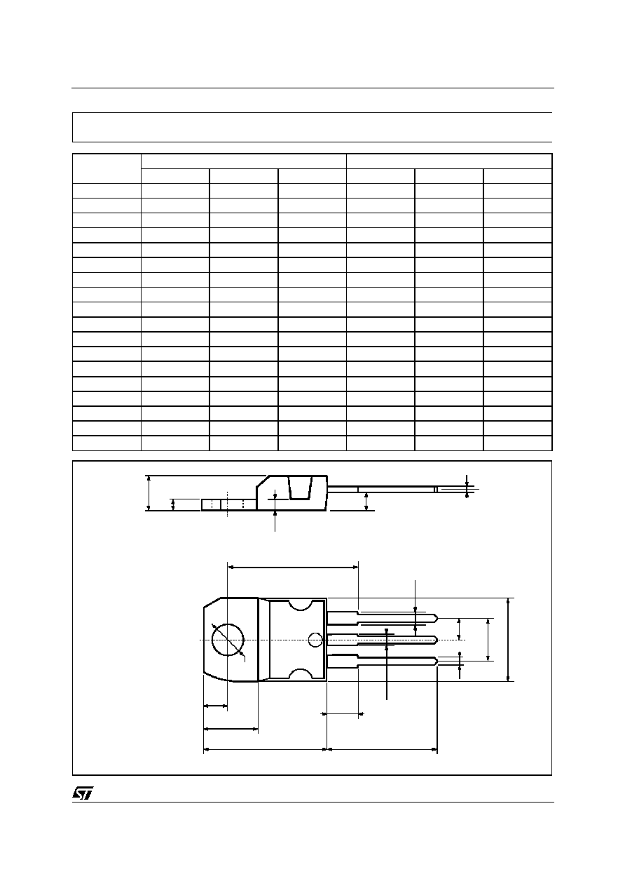
TO-220 MECHANICAL DATA
P011C
STP80NS04Z
7/8

Information furnished is believ ed to be accurate and reliable. However, STMicroelectronics assumes no responsibil ity for the consequences
of use of such information nor for any infringement of patents or other rights of third parties which may result from its use. No license is
granted by implication or otherwise under any patent or patent rights of STMicroelectronics. Specific ation mentioned in this publication are
subjec t to change without notice. This publication supersedes and replaces all information previously supplied. STMicroelectronics products
are not authorized for use as critical components in life support devices or systems without express written approval of STMicroelectronics.
The ST logo is a trademark of STMicroelectronics
©
1999 STMicroelectronics ≠ Printed in Italy ≠ All Rights Reserved
STMicroelectronics GROUP OF COMPANIES
Australia - Brazil - China - Finland - France - Germany - Hong Kong - India - Italy - Japan - Malaysia - Malta - Morocco -
Singapore - Spain - Sweden - Switzerland - United Kingdom - U.S.A.
http://www.st.com
.
STP80NS04Z
8/8