 | –≠–ª–µ–∫—Ç—Ä–æ–Ω–Ω—ã–π –∫–æ–º–ø–æ–Ω–µ–Ω—Ç: STPAC02F2 | –°–∫–∞—á–∞—Ç—å:  PDF PDF  ZIP ZIP |
May 2006
Rev 1
1/7
7
STPAC02F2
IPADTM
RF Detector for power amplifier control with internal temperature compensation
Main product characteristics
0.8 to 2.5 GHz frequency range
Detection diode voltage drop compensation
Temperature compensation
Fast response time
Low Power consumption
Chip Scale device
Low parasitic impedance
Lead free package
Description
The STPAC02F2 is an integrated RF detector for
power control chain. It has been developed to
convert the RF signal coming from the external
coupler into a DC signal usable by the mobile
digital stage. It is based on the use of two similar
diodes, one assuming the signal detection while
the second one is used to compensate the
ambient temperature effect. A biasing stage
suppresses the detection diode drop voltage
effect. The use of the IPAD technology allows the
RF front-end designer to save PCB area and to
drastically suppress the parasitic inductances of
the package.
Target applications are cellular phones and PDA
using GSM, DCS, PCS, AMPS, TDMA, CDMA
and 800 MHz to 2100 MHz frequency ranges.
Benefits
The use of IPAD technology allows the RF
front-end designer to save PCB area and to
drastically suppress the parasitic inductances.
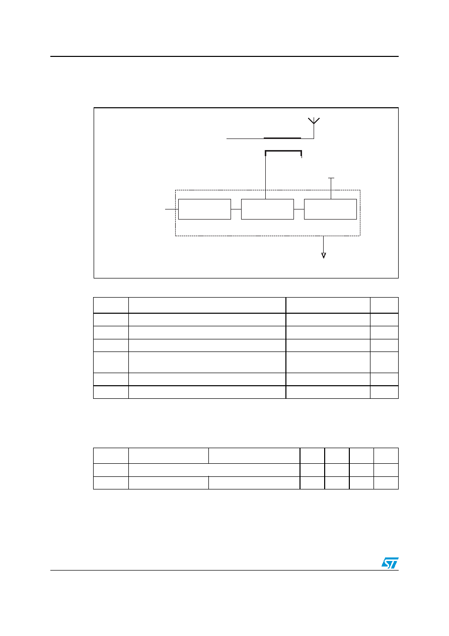
Pin configuration
Order code
Part number
Marking
STPAC02F2
RB
Flip-Chip package
(8 Bumps)
GND
RFin
GND
GND
GND
VBias
OUT
Not
used
3
2
1
A
B
C
www.st.com
Characteristics
STPAC02F2
2/7
1 Characteristics
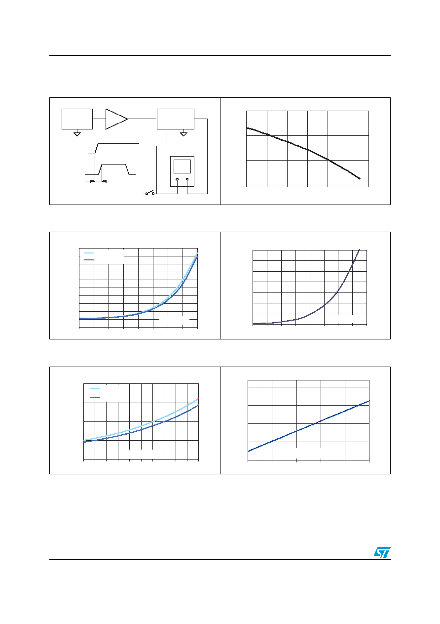
Figure 1.
Functional diagram
1.1 Electrical
characteristics
(T
amb
= 25∞ C)
Table 1.
Absolute ratings (T
amb
= 25∞ C)
Symbol
Parameter and test conditions
Value
Unit
V
BIAS
Bias voltage
5
V
P
RF
RF power at the RF input
20
dbm
F
OP
Operating frequency range
0.8 to 2.5
GHz
V
PP
ESD level as per MIL-STD 883E method 3015.7
notice 8 (HBM)
250
V
T
OP
Operating temperature range
- 30 to + 85
∞C
T
STG
Storage temperature range
- 55 to 150
∞C
Coupler
Antenna
GND
STPAC02F2
RF input
DC output
OUT
V
BIAS
Bias voltage
Low pass
filter
Thermal
compensation
RF detector
Table 2.
Parameters related to bias voltage
Symbol
Parameter
Test conditions
Min.
Typ.
Max.
Unit
V
BIAS
Operating bias voltage
2.3
2.8
3.3
V
I
BIAS
Bias current
V
BIAS
= 3.3 V
1.1
1.6
mA

STPAC02F2
Characteristics
3/7
Table 3.
Parameters related to detection function (V
BIAS
= 2.8 V,
DC output load = 200 k
)
Symbol
Parameter
Test conditions
Min
Typ
Max
Unit
V
DCout
DC output voltage
(see
Figure 2.
)
F = 1.75 GHz, P
RF
= 10 dbm
0.63
0.69
0.75
V
F = 1.75 GHz, P
RF
= - 20 dbm
0.20
0.22
0.24
F = 0.9 GHz, P
RF
= 10 dbm
0.69
0.75
0.83
F = 0.9 GHz, P
RF
= - 20 dbm
0.20
0.22
0.24
V
DCout
DC output voltage variation
(see
Figure 2.
)
2.3 V < V
BIAS
< 3.3 V,
F = 1.85 GHz, P
RF
=10 dbm
100
mV
Table 4.
Parameters related to response time (V
BIAS
= 2.8 V,
DC output load = 200 k
)
Symbol
Parameter
Test conditions
Min.
Typ.
Max.
Unit
t
VBIAS
Delay at V
BIAS
ON
(see
Figure 4.
)
V
BIAS
from 0 to 3 V
1
V
t
RFon
Delay at RF ON
(see
Figure 3.
)
P
RF
from 0 to 20 dbm
0.2
t
RFoff
Delay at RF OFF
(see
Figure 3.
)
P
RF
from 20 to 0 dbm
0.2
Figure 2.
V
DC
output measurement circuit
and temperature compensation
measurement
Figure 3.
RF Power ON/OFF response time
set-up
STPAC02
Bias voltage
OUT
RF in
RF
Generator
Power
supply
RF power amplifier
DC out
voltage
RLOAD
Climatic Chamber
-30∫C < T amb < +85∞C
STPAC02
Bias
voltage
OUT
RF in
RF
Generator
RF scope
RF power amplifier
RF in
Out
Characteristics
STPAC02F2
4/7
Figure 4.
Power supply turn ON
response time
Figure 5.
Temperature sensitivity versus RF
Power in (V
BIAS
= 2.8 V,
Freq. = 900 MHz)
STPAC02
Bias
voltage
OUT
RF in
RF
Generator
RF scope
RF power amplifier
t Pon
OUT
Bias voltage
0.0
0.1
0.2
0.3
-15
-10
-5
0
5
10
15
Delta V
(mV/∞ C)
OUT
P
(dbm)
in
Figure 6.
STPAC02 Output voltage
at wide RF power range
Figure 7.
Power detector sensitivity
at wide RF power range
0
0.2
0.4
0.6
0.8
1
1.2
1.4
1.6
1.8
2
-20
-15
-10
-5
0
5
10
15
20
900MHz
1750MHz
P
(dbm)
in
V
@ 25∞ C (V )
out
dc
0
20
40
60
80
100
120
140
-20
-15
-10
-5
0
5
10
15
20
P
(dbm)
in
Sensitivity (mV/db)
Figure 8.
STPAC02 Output voltage
at low RF power
Figure 9.
Power detector sensitivity
at low RF power
0.2
0.25
0.3
0.35
0.4
-10
-9
-8
-7
-6
-5
-4
-3
-2
-1
0
900MHz
1750MHz
P
(dbm)
in
V
@ 25∞ C (V )
out
dc
2
7
12
17
22
-10
-8
-6
-4
-2
0
2
7
12
17
22
-10
-8
-6
-4
-2
0
P
(dbm)
in
Sensitivity ( mV/db)
STPAC02F2
Packaging information
5/7
2 Packaging
information
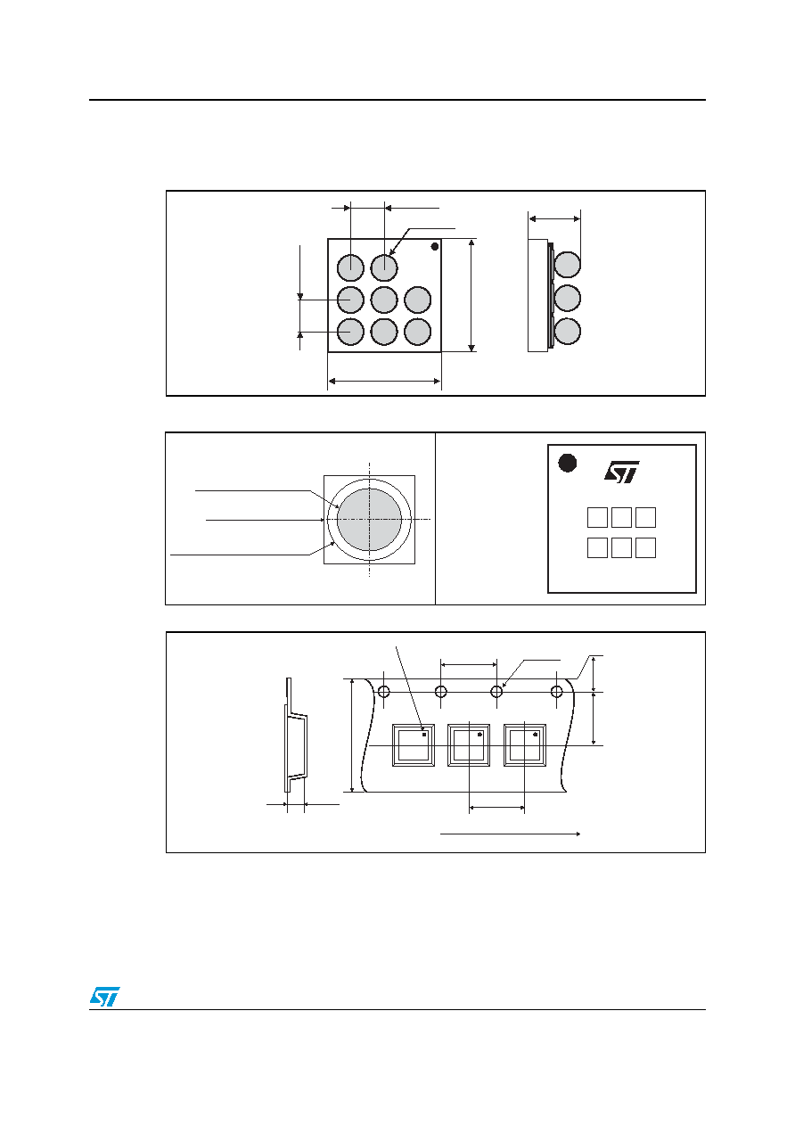
Figure 10.
Flip-Chip dimensions
Figure 13.
Flip-Chip tape and reel specification
In order to meet environmental requirements, ST offers these devices in ECOPACKÆ
packages. These packages have a lead-free second level interconnect. The category of
second level interconnect is marked on the inner box label, in compliance with JEDEC
Standard JESD97. The maximum ratings related to soldering conditions are also marked on
the inner box label. ECOPACK is an ST trademark. ECOPACK specifications are available
at: www.st.com.
Figure 11.
Foot print recommendations
Figure 12.
Marking
1.57 mm ± 50 µm
1.57 mm ± 50 µm
315 µm ± 50
500 µm ± 50
500 µm ± 50
650 µm ± 65
Copper pad Diameter:
250 µm recommended, 300 µm max
Solder stencil opening: 330 µm
Solder mask opening recommendation:
340 µm min for 300 µm copper pad diameter
x
y
x
w
z
w
Dot, ST logo
xx = marking
z = manufacturing location
yww = datecode
(y = year
ww = week)
Dot identifying Pin A1 location
User direction of unreeling
All dimensions in mm
4 +/- 0.1
8 +/- 0.3
4 +/- 0.1
1.75 +/- 0.1
3.5 +/- 0.1
ÿ 1.5 +/- 0.1
0.73 +/- 0.05
ST
xxx
yww
ST
xxx
yww
ST
xxx
yww