April 2002
1/16
Version 4.2
STV7618
PLASMA DISPLAY PANEL DATA DRIVER
FEATURES
s
96 Outputs Plasma Display Driver
s
90V Absolute Maximum Rating
s
3.3V / 5V Compatible Logic
s
-40 / 30 mA Source / Sink Output MOS
s
3 or 6 Bit Data Bus (40 MHz)
s
BCD Process
s
Packaging Adapted to Customer's Request
(DICE, COB, COF, TAB).
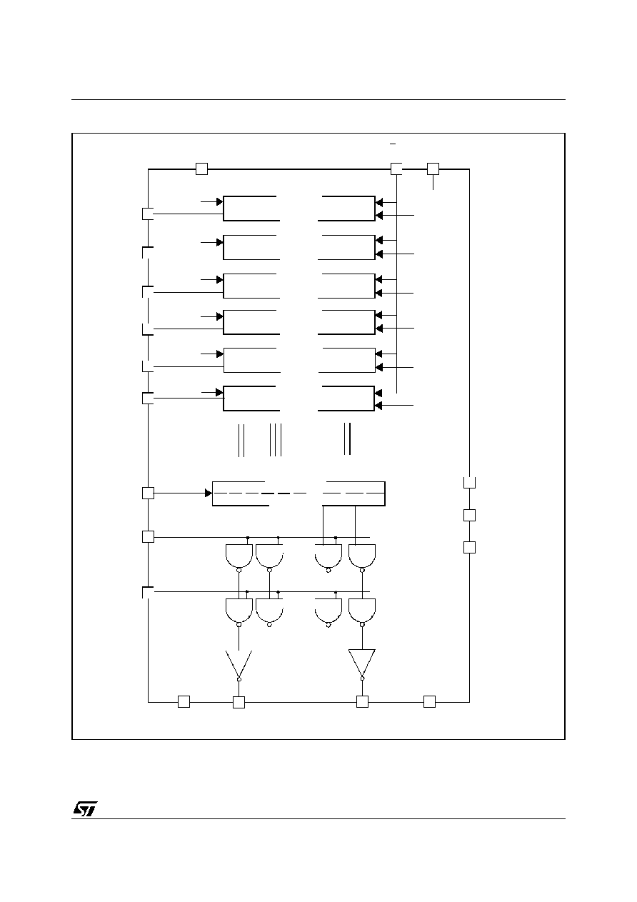
DESCRIPTION
STV7618 is a data driver for Plasma Display
Panel (PDP) designed in the ST proprietary BCD
high voltage technology. Using a 3 or 6 bit wide
data bus, it can control 96 high current & high
voltage outputs. The STV7618 is supplied with a
separated 70V power output supply and a 5V logic
supply. All command inputs are CMOS and 3.3V
logic levels compatible.
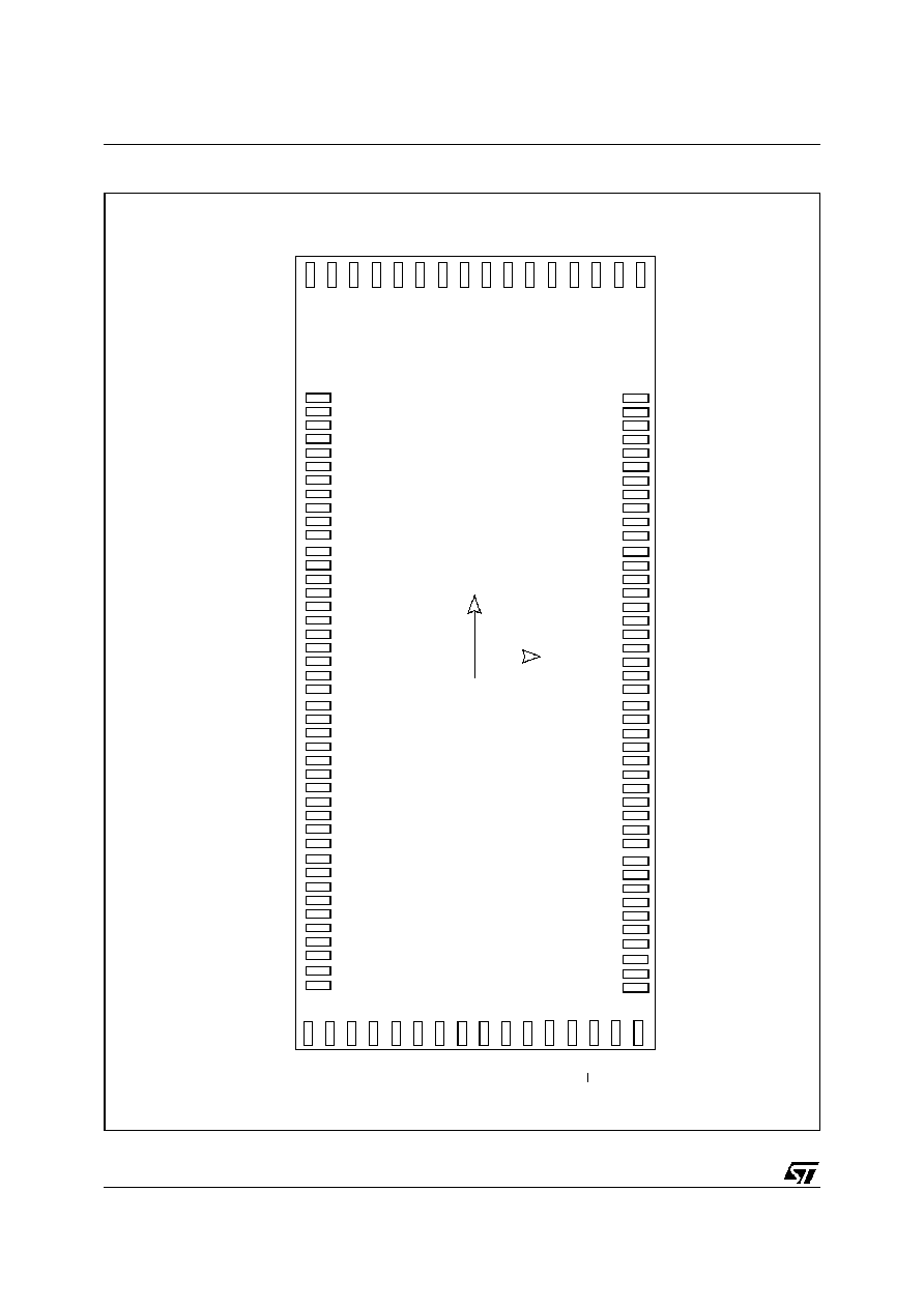
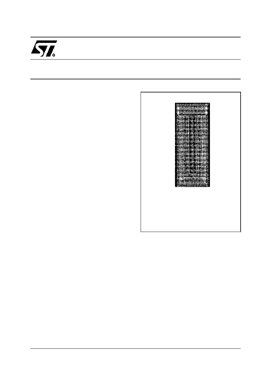
Die
ORDER CODE: STV7618/WAF (1)
(1)Unsawn tested wafer
1
STV7618
2/15
Revision follow-up
Target specification
05/2000
version 1.1
document creation
05/2000
version 1.2
few changes in figures
07/2000
version 1.3
addition of pads dimensions/coordinates,
few changes in figures and electrical characteristics
02/2001
version 1.4
TBD mentions replaced with values for Vouthl and Voutlh
Datasheet
06/2001
version 4.0
general update
10/2001
version 4.1
addition of die photo in cover page
new pads dimensions
04/2002
version 4.2
Cover page
features related to output diode current deleted
New values for Source/sink output MOS: -40/30mA
Absolute maximum ratings
I
POUT
values -150/150mA
added definition and values for I
DOUT
-200/300mA
Addition of note 4: Transient current. Spike current duration inferior to 300ns.
Tested wafer disclaimer
chapter added
2
STV7618
5/15
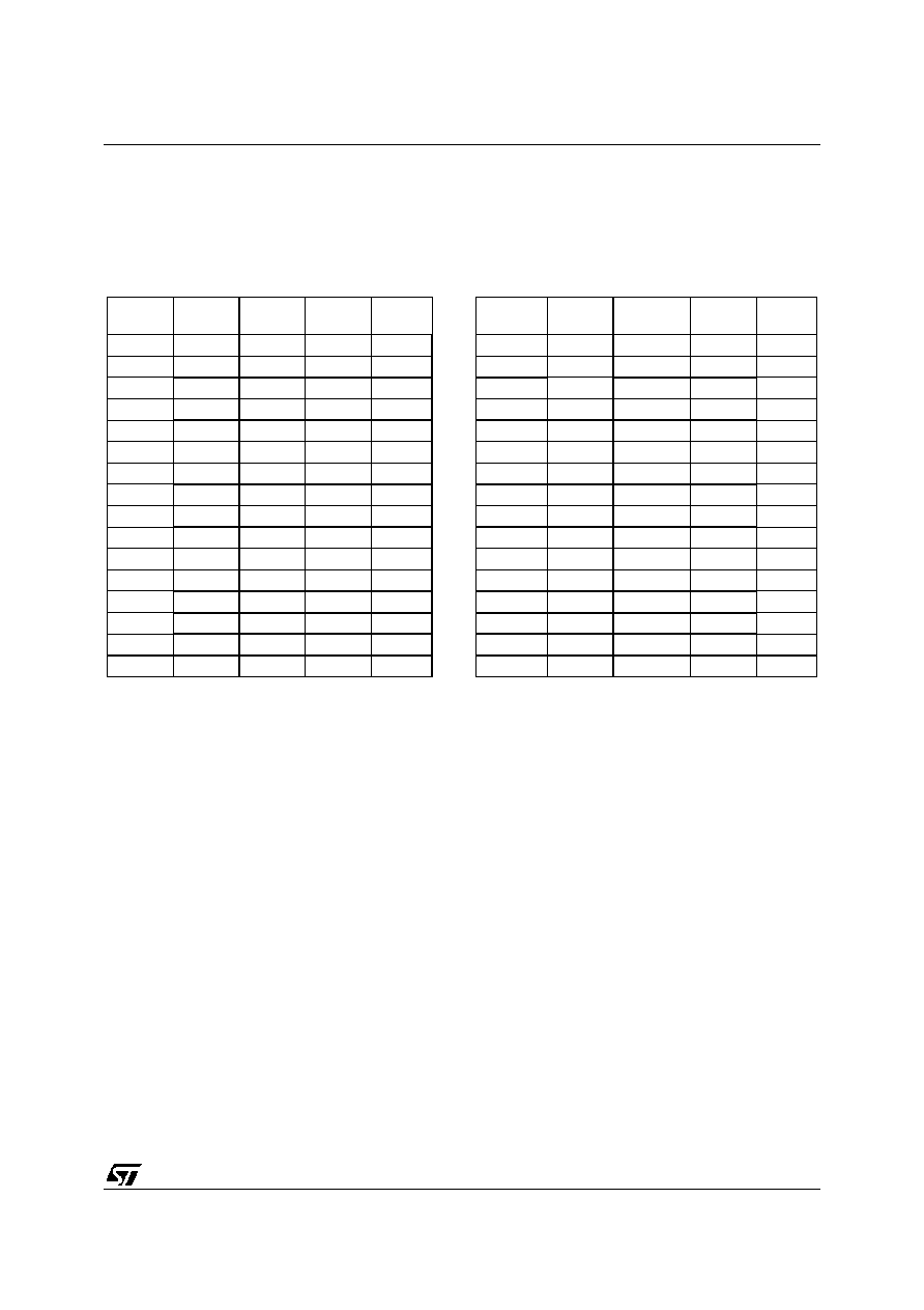
3 - PADS DIMENSIONS (in
�
m)/ PADS POSITIONS
The reference is the centre of the die (x=0, y=0)
TOP SIDE from left to right
BOTTOM SIDE from right to left
Name
Centre:
X
Centre:
Y
Size:x
SIze: y
Name
Centre:
X
Centre:Y
Size:x
SIze: y
OUT56
-774.478
2700.96
75
90
VSSLOG
773.542
-2701.045
75
90
OUT55
-671.288
2700.96
75
90
CLK
670.352
-2701.045
75
90
OUT54
-568.098
2700.96
75
90
F/R
567.162
-2701.045
75
90
OUT53
-464.907
2700.96
75
90
POC
463.972
-2701.045
75
90
OUT52
-361.718
2700.96
75
90
VCC
360.782
-2701.045
75
90
OUT51
-258.528
2700.96
75
90
STB
258.442
-2701.045
75
90
OUT50
-155.338
2700.96
75
90
BLK
155.252
-2701.045
75
90
OUT49
-52.147
2700.96
75
90
A1
52.062
-2701.045
75
90
OUT48
51.042
2700.96
75
90
A2
-51.128
-2701.045
75
90
OUT47
154.232
2700.96
75
90
A3
-154.318
-2701.045
75
90
OUT46
257.422
2700.96
75
90
A4
-257.508
-2701.045
75
90
OUT45
360.612
2700.96
75
90
A5
-360.698
-2701.045
75
90
OUT44
463.802
2700.96
75
90
A6
-463.888
-2701.045
75
90
OUT43
566.992
2700.96
75
90
VSSSUB
-567.078
-2701.045
75
90
OUT42
670.267
2700.96
75
90
BS
-670.352
-2701.045
75
90
OUT41
773.458
2700.96
75
90
VSSLOG
-773.542
-2701.045
75
90