 | –≠–ª–µ–∫—Ç—Ä–æ–Ω–Ω—ã–π –∫–æ–º–ø–æ–Ω–µ–Ω—Ç: STV7619DU | –°–∫–∞—á–∞—Ç—å:  PDF PDF  ZIP ZIP |
Æ
August 2003
1/21
STV7619DU
Scan Driver for Plasma Display Panels
Main Features
s
64-output Scan Driver
s
120 V Absolute Maximum Supply
s
5 V Logic Supply
s
Optional 12 V Supply for driving the output
stage
s
150mA/1A Source/Sink Output
s
1 A Source/Sink Output Diode
s
64-bit Bi-directional Shift Register (8 MHz)
s
BCD Technology
s
100-pin TQFP package with integrated
heatsink
Description
The STV7619 is a scan driver for plasma display
panels (PDP) implemented in ST's proprietary BCD
(Bi-polar CMOS DMOS) technology. Using a 64-bit
cascadable 8 MHz shift register, it drives 64 high-
current and high-voltage outputs.
By connecting several STV7619 devices in series,
any vertical pixel definition can be performed. The
STV7619 is supplied with separate 110V power
output and 5 V logic supplies. The logic section of
the output stage is supplied either externally by a
5V or 12V supply or internally by a charge pump
cell. The choice of the supply value is related to the
PDP size. All command inputs are CMOS
compatible.
The STV7619 package is a 100-pin TQFP with
integrated heatsink located on the bottom
(STV7619D) of the package. It is also available
without heatsink (STV7619).
TQFP100 (14 x 14 x 1.4 mm Slug-down)
(Thin Plastic Quad Flat Pack)
ORDER CODE: STV7619D
TQFP100 (14 x 14 x 1.4 mm)
(Thin Plastic Quad Flat Pack)
ORDER CODE: STV7619

2/21
STV7619DU
Table of Contents
Chapter 1
Pin Allocation and Descriptions . . . . . . . . . . . . . . . . . . . . . . . . . . . . . . . . . . . . . .3
1.1
Pinout Diagrams ............................................................................................................... 3
Chapter 2
Circuit Description . . . . . . . . . . . . . . . . . . . . . . . . . . . . . . . . . . . . . . . . . . . . . . . . .7
Chapter 3
Application Hints: Charge Pump Function . . . . . . . . . . . . . . . . . . . . . . . . . . . . .9
3.1
Power Supply ....................................................................................................................... 9
3.2
Sink Current Characteristics .............................................................................................. 10
3.3
Recommendations ............................................................................................................. 10
Chapter 4
Electrical Characteristics . . . . . . . . . . . . . . . . . . . . . . . . . . . . . . . . . . . . . . . . . .11
4.1
Absolute Maximum Ratings .............................................................................................. 11
4.2
Thermal Data .................................................................................................................... 12
4.3
Supply Characteristics ....................................................................................................... 12
4.4
Power Output Characteristics ........................................................................................... 13
4.5
SOUT Characteristics ....................................................................................................... 14
4.6
Input (CLK, STB, BLK, POC, SIN, CLR, F/R and ENABLE) Characteristics .................... 14
4.7
AC Timing Requirements ................................................................................................... 14
4.8
AC Timing Characteristics ................................................................................................. 15
Chapter 5
Input/Output Schematic Diagrams . . . . . . . . . . . . . . . . . . . . . . . . . . . . . . . . . . .18
Chapter 6
Package Mechanical Data . . . . . . . . . . . . . . . . . . . . . . . . . . . . . . . . . . . . . . . . .19
Chapter 7
Revision History . . . . . . . . . . . . . . . . . . . . . . . . . . . . . . . . . . . . . . . . . . . . . . . . . .20

Pin Allocation and Descriptions
STV7619DU
3/21
1
Pin Allocation and Descriptions
1.1
Pinout Diagrams
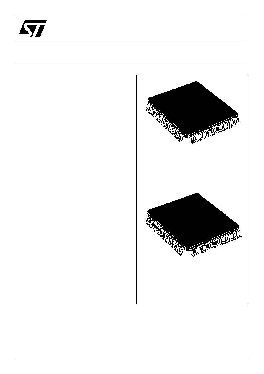
Figure 1: STV7619 and STV7619D (TQFP100)
1
2
3
4
5
6
7
8
9
10
11
12
13
14
15
16
17
18
19
20
21
22
23
24
25
75
74
73
72
71
70
69
68
67
66
65
64
63
62
61
60
59
58
57
56
55
54
53
52
51
26
27
28
29
30
31
32
33
34
35
36
37
38
39
40
41
42
43
44
45
46
47
48
49
50
10
0
99
98
97
96
95
94
93
92
91
90
89
88
87
86
85
84
83
82
81
80
79
78
77
76
OUT61
OUT60
OUT59
OUT58
OUT57
OUT56
OUT55
OUT54
OUT53
OUT52
OUT51
OUT50
OUT49
OUT48
OUT47
OUT46
OUT45
OUT44
OUT43
OUT42
OUT41
OUT40
OUT39
OUT4
OUT5
OUT6
OUT7
OUT8
OUT9
OUT10
OUT11
OUT12
OUT13
OUT14
OUT15
OUT16
OUT17
OUT18
OUT19
OUT20
OUT21
OUT22
OUT23
OUT24
OUT25
OUT26
OUT27
OUT28
OU
T
3
2
OU
T
6
4
NC
*
SO
U
T
CL
K
ST
B
BL
K
PO
C
CL
R
NC
*
OU
T
2
OU
T
3
TQFP100
(Top View)
OU
T
1
OU
T
6
3
OU
T
6
2
OUT38
OUT37
OU
T
3
6
OU
T
3
3
OU
T
3
4
OU
T
3
5
OU
T
3
1
OU
T
3
0
OU
T
2
9
VPP
VS
SP
VS
SP
NC*
NC
*
VS
SL
O
G
VSSL
O
G
VSSSUB
VPP
VPP
NC
*
VS
SP
VS
SP
VP
P
VP
P
V
SSP
V
SSP
VDD
SI
N
VC
C
F/
R
V
SSL
O
G
V
SSP
V
SSP
*NC: Not Connected
E
N
ABL
E
VSSSU
B
VPP
NC
*

4/21
STV7619DU
Pin Allocation and Descriptions
Table 1: Supply Pins
Pin No.
Pin Name
Pin Description
88
VCC
5V Logic Supply
84
VDD
5/12V Internal/External Logic Supply
33
VPP
High Voltage Supply for Power Outputs
34
VPP
High Voltage Supply for Power Outputs
42
VPP
High Voltage Supply for Power Outputs
43
VPP
High Voltage Supply for Power Outputs
79
VPP
High Voltage Supply for Power Outputs
97
VPP
High Voltage Supply for Power Outputs
36
VSSLOG
Logic Ground
40
VSSLOG
Logic Ground
83
VSSLOG
Logic Ground
30
VSSP
Ground for Power Outputs
31
VSSP
Ground for Power Outputs
45
VSSP
Ground for Power Outputs
46
VSSP
Ground for Power Outputs
81
VSSP
Ground for Power Outputs
82
VSSP
Ground for Power Outputs
94
VSSP
Ground for Power Outputs
95
VSSP
Ground for Power Outputs
37
VSSSUB
Substrate Ground
39
VSSSUB
Substrate Ground
Table 2: Shift Register and Input Pins
Pin No.
Pin Name
Pin Description
38
ENABLE
Enable Charge Pump mode
85
SOUT
Shift Register Data Output
86
CLK
Clock for Shift Register Data
87
STB
Latch for Shift Register Data (Strobe Input)
89
BLK
Blanking Control for Power Outputs
90
POC
Polarity Output Control
91
SIN
Shift Register Data Input
92
CLR
Clear for Shift Register Data
93
F/R
Foward/Reserve modes for selecting Shift Register
Pin Allocation and Descriptions
STV7619DU
5/21
Table 3: Power Output Pins
Pin No.
Pin Name
Pin Description
Pin No.
Pin Name
Pin Description
98
OUT1
Power Output 1
47
OUT33
Power Output 33
99
OUT2
Power Output 2
48
OUT34
Power Output 34
100
OUT3
Power Output 3
49
OUT35
Power Output 35
1
OUT4
Power Output 4
50
OUT36
Power Output 36
2
OUT5
Power Output 5
51
OUT37
Power Output 37
3
OUT6
Power Output 6
52
OUT38
Power Output 38
4
OUT7
Power Output 7
53
OUT39
Power Output 39
5
OUT8
Power Output 8
54
OUT40
Power Output 40
6
OUT9
Power Output 9
55
OUT41
Power Output 41
7
OUT10
Power Output 10
56
OUT42
Power Output 42
8
OUT11
Power Output 11
57
OUT43
Power Output 43
9
OUT12
Power Output 12
58
OUT44
Power Output 44
10
OUT13
Power Output 13
59
OUT45
Power Output 45
11
OUT14
Power Output 14
60
OUT46
Power Output 46
12
OUT15
Power Output 15
61
OUT47
Power Output 47
13
OUT16
Power Output 16
62
OUT48
Power Output 48
14
OUT17
Power Output 17
63
OUT49
Power Output 49
15
OUT18
Power Output 18
64
OUT50
Power Output 50
16
OUT19
Power Output 19
65
OUT51
Power Output 51
17
OUT20
Power Output 20
66
OUT52
Power Output 52
18
OUT21
Power Output 21
67
OUT53
Power Output 53
19
OUT22
Power Output 22
68
OUT54
Power Output 54
20
OUT23
Power Output 23
69
OUT55
Power Output 55
21
OUT24
Power Output 24
70
OUT56
Power Output 56
22
OUT25
Power Output 25
71
OUT57
Power Output 57
23
OUT26
Power Output 26
72
OUT58
Power Output 58
24
OUT27
Power Output 27
73
OUT59
Power Output 59
25
OUT28
Power Output 28
74
OUT60
Power Output 60
26
OUT29
Power Output 29
75
OUT61
Power Output 61
27
OUT30
Power Output 30
76
OUT62
Power Output 62
28
OUT31
Power Output 31
77
OUT63
Power Output 63
29
OUT32
Power Output 32
78
OUT64
Power Output 64