1/9
June 2004
STW30NM60D
N-CHANNEL 600V - 0.125
- 30A TO-247
Fast Diode MDmeshTM MOSFET
Table 1: General Features
s
TYPICAL R
DS
(on) = 0.125
s
HIGH dv/dt AND AVALANCHE CAPABILITIES
s
100% AVALANCHE RATED
s
LOW INPUT CAPACITANCE AND GATE
CHARGE
s
LOW GATE INPUT RESISTANCE
s
FAST INTERNAL RECOVERY DIODE
DESCRIPTION
The FDmeshTM
associates all advantages of re-
duced on-resistance and fast switching with an in-
trinsic fast-recovery body diode. It is therefore
strongly recommended for bridge topologies, in
particular ZVS phase-shift converters.
APPLICATIONS
s
ZVS PHASE-SHIFT FULL BRIDGE
CONVERTERS FOR SMPS AND WELDING
EQUIPMENT
Table 2: Order Codes
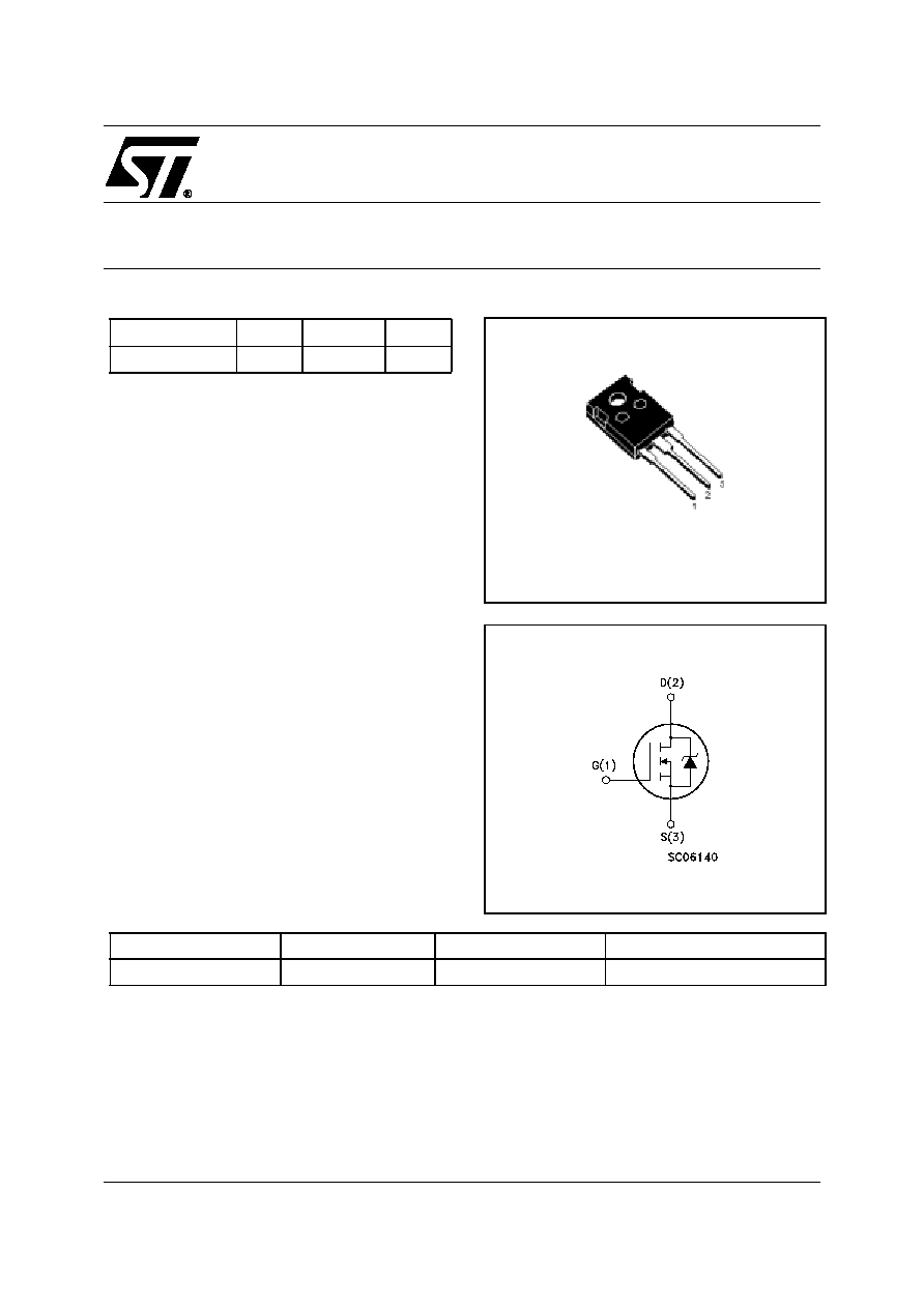
Figure 1: Package
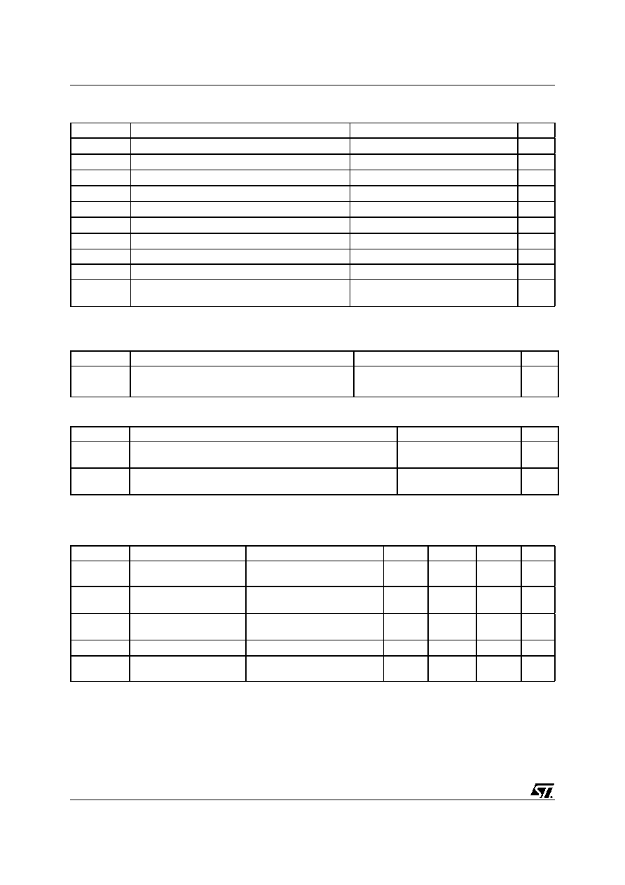
Figure 2: Internal Schematic Diagram
TYPE
V
DSS
R
DS(on)
I
D
STW30NM60D
600 V
< 0.145
30 A
TO-247
SALES TYPE
MARKING
PACKAGE
PACKAGING
STW30NM60D
W30NM60D
TO-247
TUBE
Rev. 3
STW30NM60D
2/9
Table 3: Absolute Maximum ratings
( ) Pulse width limited by safe operating area
(1) I
SD
30A, di/dt
400A/µs, V
DD
V
(BR)DSS
, T
j
T
JMAX.
Table 4: Thermal Data
Table 5: Avalanche Characteristics
ELECTRICAL CHARACTERISTICS (T
CASE
=25∞C UNLESS OTHERWISE SPECIFIED)
Table 6: On /Off
Symbol
Parameter
Value
Unit
V
DS
Drain-source Voltage (V
GS
= 0)
600
V
V
DGR
Drain-gate Voltage (R
GS
= 20 k
)
600
V
V
GS
Gate- source Voltage
± 30
V
I
D
Drain Current (continuous) at T
C
= 25∞C
30
A
I
D
Drain Current (continuous) at T
C
= 100∞C
18.9
A
I
DM
( )
Drain Current (pulsed)
120
A
P
TOT
Total Dissipation at T
C
= 25∞C
312
W
Derating Factor
2.5
W/∞C
dv/dt (1)
Peak Diode Recovery voltage slope
20
V/ns
T
j
T
stg
Operating Junction Temperature
Storage Temperature
-55 to 150
-55 to 150
∞C
∞C
Rthj-case
Thermal Resistance Junction-case Max
0.4
∞C/W
Rthj-amb
Thermal Resistance Junction-ambient Max
62.5
∞C/W
T
l
Maximum Lead Temperature For Soldering Purpose
300
∞C
Symbol
Parameter
Max Value
Unit
I
AR
Avalanche Current, Repetitive or Not-Repetitive
(pulse width limited by T
j
max)
15
A
E
AS
Single Pulse Avalanche Energy
(starting T
j
= 25 ∞C, I
D
= I
AR
, V
DD
= 50 V)
740
mJ
Symbol
Parameter
Test Conditions
Min.
Typ.
Max.
Unit
V
(BR)DSS
Drain-source Breakdown
Voltage
I
D
= 1 mA, V
GS
= 0
600
V
I
DSS
Zero Gate Voltage
Drain Current (V
GS
= 0)
V
DS
= Max Rating
V
DS
= Max Rating, T
C
= 125∞C
10
100
µA
µA
I
GSS
Gate-body Leakage
Current (V
DS
= 0)
V
GS
= ± 20 V
± 10
µA
V
GS(th)
Gate Threshold Voltage
V
DS
= V
GS
, I
D
= 250 µA
3
4
5
V
R
DS(on
Static Drain-source On
Resistance
V
GS
= 10 V, I
D
= 15 A
0.125
0.145
3/9
STW30NM60D
Table 7: Dynamic
Table 8: Source Drain Diode
(1) Pulsed: Pulse duration = 300 µs, duty cycle 1.5 %.
(2) Pulse width limited by safe operating area.
(3) C
oss eq.
is defined as a constant equivalent capacitance giving the same charging time as C
oss
when V
DS
increases from 0 to 80% V
DSS
.
Symbol
Parameter
Test Conditions
Min.
Typ.
Max.
Unit
g
fs
(1)
Forward Transconductance
V
DS
= 15 V , I
D
= 15 A
16
S
C
iss
C
oss
C
rss
Input Capacitance
Output Capacitance
Reverse Transfer
Capacitance
V
DS
= 25 V, f = 1 MHz,
V
GS
= 0
2520
800
75
pF
pF
pF
C
OSS eq
(3)
.
Equivalent Output
Capacitance
V
GS
= 0 V, V
DS
= 0 to 480 V
390
pF
t
d(on)
t
r
t
d(off)
t
f
Turn-on Delay Time
Rise Time
Turn-off-Delay Time
Fall Time
V
DD
= 300 V, I
D
= 15 A,
R
G
= 4.7
,
V
GS
= 10 V
(see Figure 15)
32
33
75
35
ns
ns
ns
ns
Q
g
Q
gs
Q
gd
Total Gate Charge
Gate-Source Charge
Gate-Drain Charge
V
DD
= 480 V, I
D
= 30 A,
V
GS
= 10 V
(see Figure 18)
82
24
42
115
nC
nC
nC
Symbol
Parameter
Test Conditions
Min.
Typ.
Max.
Unit
I
SD
I
SDM
(2)
Source-drain Current
Source-drain Current (pulsed)
30
120
A
A
V
SD
(1)
Forward On Voltage
I
SD
= 30 A, V
GS
= 0
1.5
V
t
rr
Q
rr
I
RRM
Reverse Recovery Time
Reverse Recovery Charge
Reverse Recovery Current
I
SD
= 30 A, di/dt = 100 A/µs
V
DD
= 50V
(see Figure 16)
165
1.1
14
ns
nC
A
t
rr
Q
rr
I
RRM
Reverse Recovery Time
Reverse Recovery Charge
Reverse Recovery Current
I
SD
= 30 A, di/dt = 100 A/µs
V
DD
= 50V, T
j
= 150∞C
(see Figure 16)
312
3.3
21
ns
nC
A
STW30NM60D
4/9
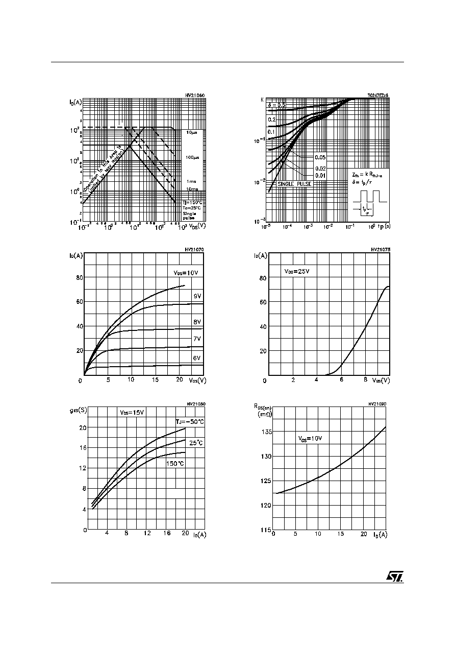
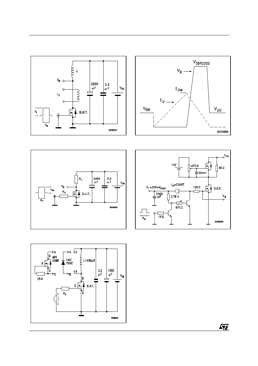
Figure 3: Safe Operating Area
Figure 4: Output Characteristics
Figure 5: Transconductance
Figure 6: Thermal Impedance
Figure 7: Transfer Characteristics
Figure 8: Static Drain-source On Resistance
5/9
STW30NM60D
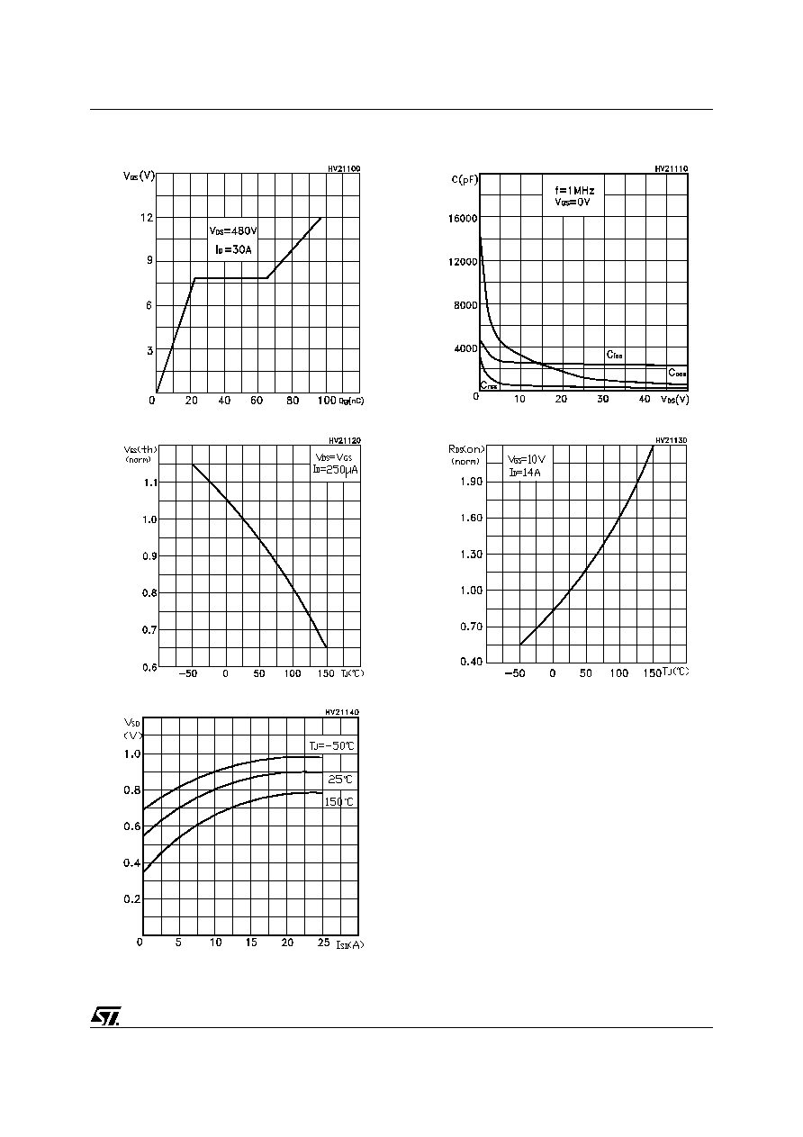
Figure 9: Gate Charge vs Gate-source Voltage
Figure 10: Normalized Gate Thereshold Volt-
age vs Temperature
Figure 11: Dource-Drain Diode Forward Char-
acteristics
Figure 12: Capacitance Variations
Figure 13: Normalized On Resistance vs Tem-
perature
STW30NM60D
6/9
Figure 14: Unclamped Inductive Load Test Cir-
cuit
Figure 15: Switching Times Test Circuit For
Resistive Load
Figure 16: Test Circuit For Inductive Load
Switching and Diode Recovery Times
Figure 17: Unclamped Inductive Wafeform
Figure 18: Gate Charge Test Circuit

7/9
STW30NM60D
DIM.
mm.
inch
MIN.
TYP
MAX.
MIN.
TYP.
MAX.
A
4.85
5.15
0.19
0.20
A1
2.20
2.60
0.086
0.102
b
1.0
1.40
0.039
0.055
b1
2.0
2.40
0.079
0.094
b2
3.0
3.40
0.118
0.134
c
0.40
0.80
0.015
0.03
D
19.85
20.15
0.781
0.793
E
15.45
15.75
0.608
0.620
e
5.45
0.214
L
14.20
14.80
0.560
0.582
L1
3.70
4.30
0.14
0.17
L2
18.50
0.728
¯P
3.55
3.65
0.140
0.143
¯R
4.50
5.50
0.177
0.216
S
5.50
0.216
TO-247 MECHANICAL DATA

STW30NM60D
8/9
Table 9: Revision History
Date
Revision
Description of Changes
24-June-2004
3
The document change from "ADVANCED" to "COMPLETE".
New Stylesheet.
Rds(on) Max@10V changed. See Table 6.

9/9
STW30NM60D
Information furnished is believed to be accurate and reliable. However, STMicroelectronics assumes no responsibility for the
consequences of use of such information nor for any infringement of patents or other rights of third parties which may result from
its use. No license is granted by implication or otherwise under any patent or patent rights of STMicroelectronics. Specifications
mentioned in this publication are subject to change without notice. This publication supersedes and replaces all information
previously supplied. STMicroelectronics products are not authorized for use as critical components in life support devices or
systems without express written approval of STMicroelectronics.
The ST logo is a registered trademark of STMicroelectronics
All other names are the property of their respective owners
© 2004 STMicroelectronics - All Rights Reserved
STMicroelectronics GROUP OF COMPANIES
Australia - Belgium - Brazil - Canada - China - Czech Republic - Finland - France - Germany - Hong Kong - India - Israel - Italy - Japan -
Malaysia - Malta - Morocco - Singapore - Spain - Sweden - Switzerland - United Kingdom - United States.