 | ÐлекÑÑоннÑй компоненÑ: TGA8652 | СкаÑаÑÑ:  PDF PDF  ZIP ZIP |
TGA8652-EPU Datasheet PDF

TriQuint Semiconductor Texas : (972)994 8465 Fax (972)994 8504 Web: www.triquint.com
Advance Product Datasheet
1
DC-18GHz MPA with AGC TGA8652-EPU
OC-192 12.5Gb/s LN/MZ Driver and Receive AGC Applications
Surface Mount Package
Key Features and Performance
·
0.5um pHEMT Dual Gate Technology
·
DC - 14GHz Linear BW
·
DC - 18GHz Saturated Power BW
·
16dB small signal gain
·
6 dB AGC Range
·
25ps Edge Rates (10/90)
·
8Vpp 12.5Gb/s NRZ PRBS
·
Low Power Dissipation
·
Package size: .350 x .350 x .084 inches.
·
Evaluation Board Available.
Primary Applications
·
12.5Gb/s NRZ Modulator Driver
·
Receiver AGC
Description
The TriQuint TGA8652EPU is a medium power wideband
AGC amplifier combined with off chip circuitry assembled
in a Surface Mount Package. The TGA8652EPU typically
provides 16dB small signal gain with 6dB AGC range.
Typical input and output return loss is <10dB. Typical
Noise Figure is 2.5dB at 3GHz. Typical saturated output
power is 25dBm. Small signal 3dB BW is 14GHz with
saturated power performance to 18GHz. RF ports are DC
coupled enabling the user to customize system corner
frequencies. Applications include OC192 12.5GBit/s NRZ
Lithium Niobate Modulator and receive AGC amplifier.
Drain bias may be applied thru the on-chip drain
termination resistor for low drive applications or thru the
RF output port for high drive applications. A cascaded
pair demonstrated 8Vpp output voltage swing with
500mVpp at the input when stimulated with 10GBit/s.
2^31-1prbs. NRZ data.
The TGA8652EPU is available on an evaluation board.
November 14. 2001
Note: Devices designated as EPU are typically early in their characterization process prior to finalizing all electrical and process
specifications. Specifications are subject to change without notice.
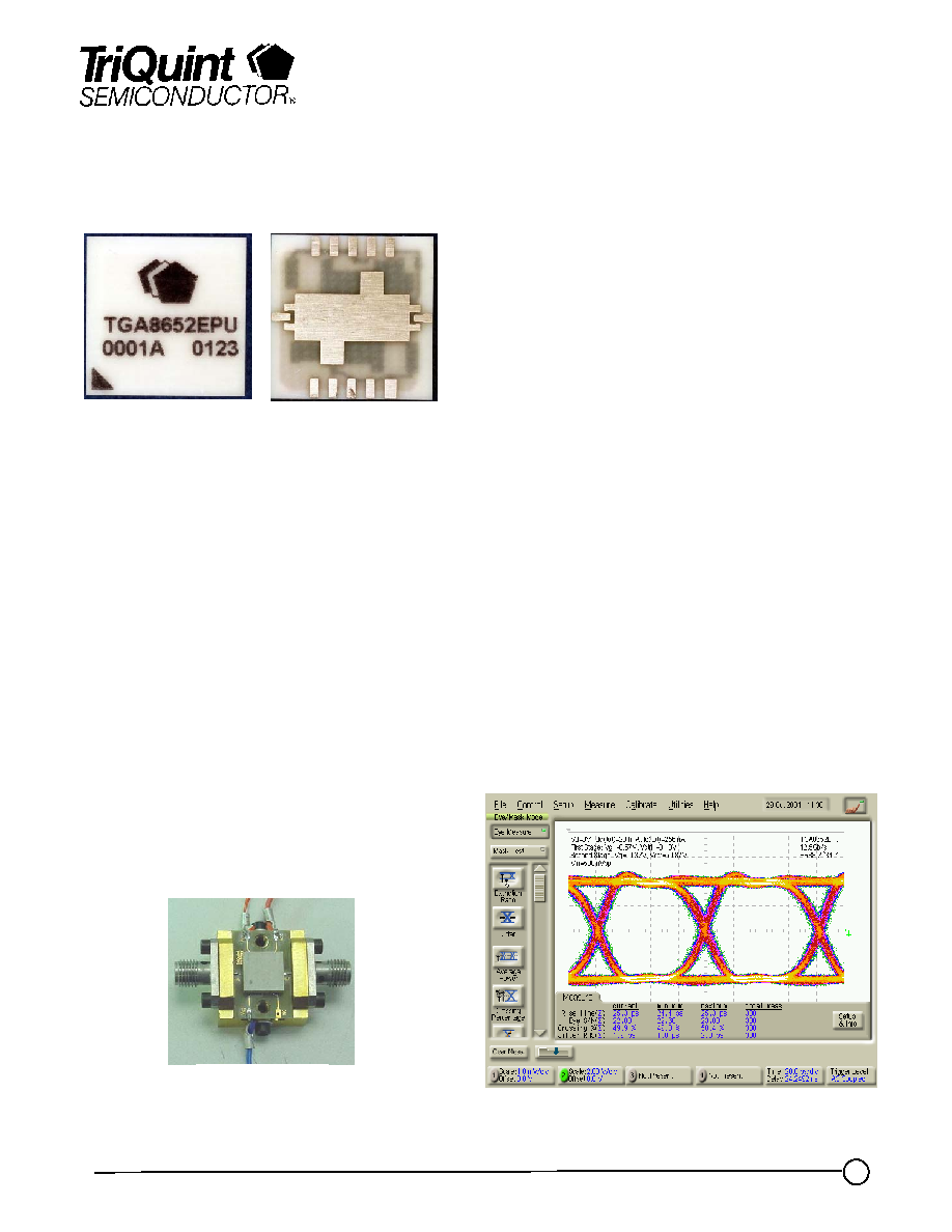
Cascaded 8652 Evaluation Boards
12.5Gb/s Performance
Output = 8Vpp, Input = 500mVpp
Scale: 2V/div, 20ps/div
Measured Performance
Bottom View
Top View
Evaluation Board

TriQuint Semiconductor Texas : (972)994 8465 Fax (972)994 8504 Web: www.triquint.com
Advance Product Datasheet
2
MAXIMUM RATINGS
SYMBOL
PARAMETER 5/
VALUE
NOTES
V
+
POSITIVE SUPPLY VOLTAGE
10 V
I
+
POSITIVE SUPPLY CURRENT
250 mA
1/
P
IN
INPUT CONTINUOUS WAVE POWER
23 dBm
4/
P
D
POWER DISSIPATION
2.6 W
T
CH
OPERATING CHANNEL TEMPERATURE
150
0
C
2/ 3/
T
STG
STORAGE TEMPERATURE
-20 to 150
0
C
1/
Total current .
2/
These ratings apply to each individual FET.
3/
Junction operating temperature directly affects the device median time to failure (T
M
). For maximum life and
best performance, it is recommended that junction temperatures be maintained at the lowest possible levels.
4/
This value reflects an estimate.
5/
These ratings represent the maximum operable values for the device.
Note: Devices designated as EPU are typically early in their characterization process prior to finalizing all electrical and process
specifications. Specifications are subject to change without notice.
TGA8652-EPU
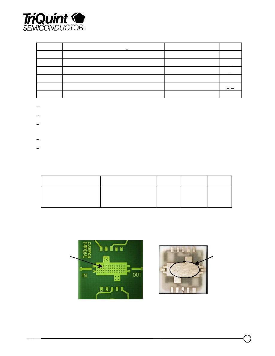
NOTE: Thermal transfer is conducted thru the bottom of the TGA8652-EPU package into
the motherboard. Design the motherboard to assure adequate thermal transfer to the base
plate. An array of filled thermal vias is recommended as shown in the example below.
Parameter
Test Condition
T
CH
(
°
C)
R
JC
(
°
C/W)
T
M
(HRS)
R
JC
Thermal Resistance
(channel to backside of package)
Vdfet = 6 V, V
ctrl
= 1 V,
I
D
= 170 mA
±
5%
115
45
> 1E+7
THERMAL INFORMATION
Thermal vias in
motherboard
Bottom View
TGA8652EPU
Area of thermal
transfer.
Motherboard

TriQuint Semiconductor Texas : (972)994 8465 Fax (972)994 8504 Web: www.triquint.com
Advance Product Datasheet
3
Note: Devices designated as EPU are typically early in their characterization process prior to finalizing all electrical and process
specifications. Specifications are subject to change without notice.
TGA8652-EPU
RF SPECIFICATIONS
(T
A
= 25
°
C + 5
°
C)
NOTE
TEST
MEASUREMENT
CONDITIONS
VALUE
UNITS
8V @ 175mA
MIN
TYP
MAX
1/
SMALL SIGNAL BANDWIDTH
12
GHz
SATURATED POWER BW
18
GHz
1/
SMALL-SIGNAL
GAIN MAGNITUDE
2.5GHz
16
dB
AGC RANGE
Midband
6
dB
NOISE FIGURE
3GHz
2.5
dB
SATURATED OUTPUT
VOLTAGE
10Gb/s with Vin-2Vpp
8
Vpp
1/
SATURATED OUTPUT
POWER
DC-10GHz
25
dBm
2/
INPUT RETURN LOSS
MAGNITUDE
DC-10GHz
-12
dB
2/
OUTPUT RETURN LOSS
MAGNITUDE
DC-10GHz
-12
dB
GROUP DELAY
DC-10GHz
+/- 20
ps
RISE TIME
< 30
ps
Notes:
1/ Measured at wafer RF probe
2/ Measured at package RF probe

TriQuint Semiconductor Texas : (972)994 8465 Fax (972)994 8504 Web: www.triquint.com
Advance Product Datasheet
4
Note: Devices designated as EPU are typically early in their characterization process prior to finalizing all electrical and process
specifications. Specifications are subject to change without notice.
TGA8652-EPU
0
2
4
6
8
10
12
14
16
18
20
2
4
6
8
10
12
14
16
18
20
Frequency (GHz)
S21 (
d
B
)
-45
-40
-35
-30
-25
-20
-15
-10
-5
0
2
4
6
8
10
12
14
16
18
20
Frequency (GHz)
S11 (
d
B
)
an
d
S22 (
d
B
)
s11
s22
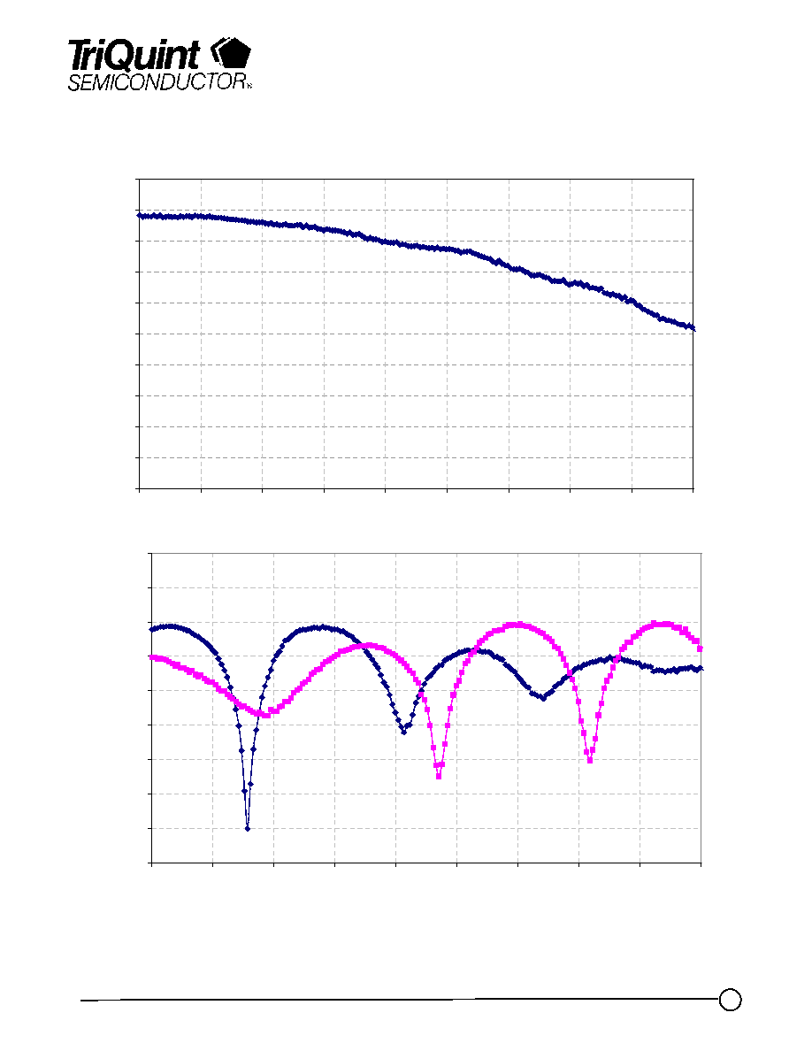
TGA8652 Typical Measured S-parameters

TriQuint Semiconductor Texas : (972)994 8465 Fax (972)994 8504 Web: www.triquint.com
Advance Product Datasheet
5
Note: Devices designated as EPU are typically early in their characterization process prior to finalizing all electrical and process
specifications. Specifications are subject to change without notice.
TGA8652-EPU
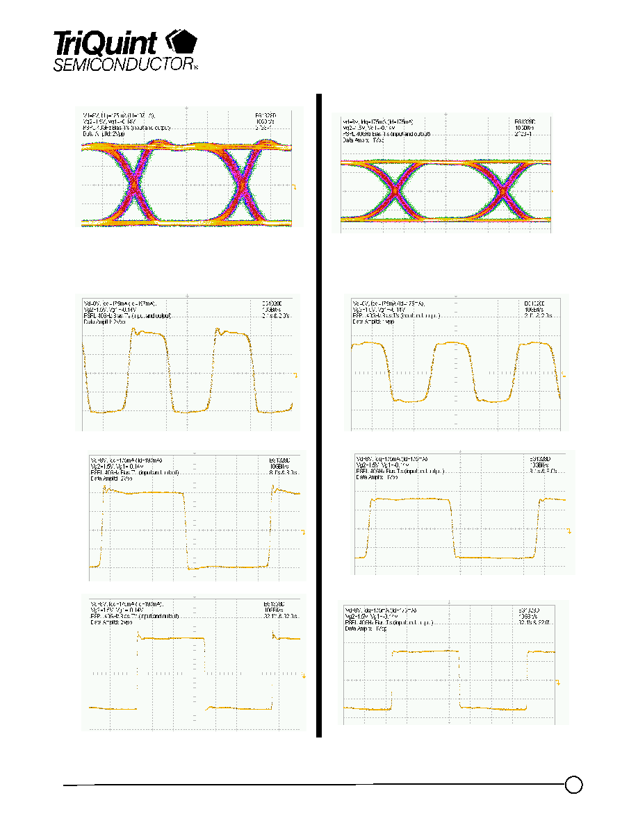
10GBit/s Performance
Output = 8V P-P, Input = 2V P-P
scale 2V/div, 20ps/div
10GBit/s Performance
Output =6V P-P, Input = 1V P-P
scale 2V/div, 20ps/div
Measured Performance
2 1's and 2 0's, 100ps/div
8 1's and 8 0's, 200ps/div
32 1's and 32 0's, 1ns/div
8V P-P (Saturated)
6V P-P (Near Small Signal)
8V P-P
6V P-P
2 1's and 2 0's, 100ps/div
8 1's and 8 0's, 200ps/div
32 1's and 32 0's, 1ns/div
