 | –≠–ª–µ–∫—Ç—Ä–æ–Ω–Ω—ã–π –∫–æ–º–ø–æ–Ω–µ–Ω—Ç: L2949E | –°–∫–∞—á–∞—Ç—å:  PDF PDF  ZIP ZIP |
UTC L2949E
LINEAR INTEGRATED CIRCUIT
UTC
UNISONIC TECHNOLOGIES CO. LTD
1
QW-R102-014,A
MULTIFUNCTION VERY LOW
DROP VOLTAGE REGULATOR
DESCRIPTION
The UTC L2949E is a monolithic integrated 5V voltage
regulator with a very low dropout output and additonal
functions as power-on reset and input voltage sense.It is
designed for supplying the microcomputer controlled
systems especially in automotive applications.
FEATURES
*Operating dc supply voltage range 5V to 28V.
*Transient supply voltage up to 40V.
*Extremely low quiescent current in standby mode.
*High precision standby output voltage 5V±1%
*Output current capability up to 100mA.
*Very low dropout voltage less than 0.5V.
*Reset circuit sensing the output voltage
*Programmable reset pulse delay with external capacitor
*Voltage sense comparator.
*Thermal shutdown and short circuit protections.
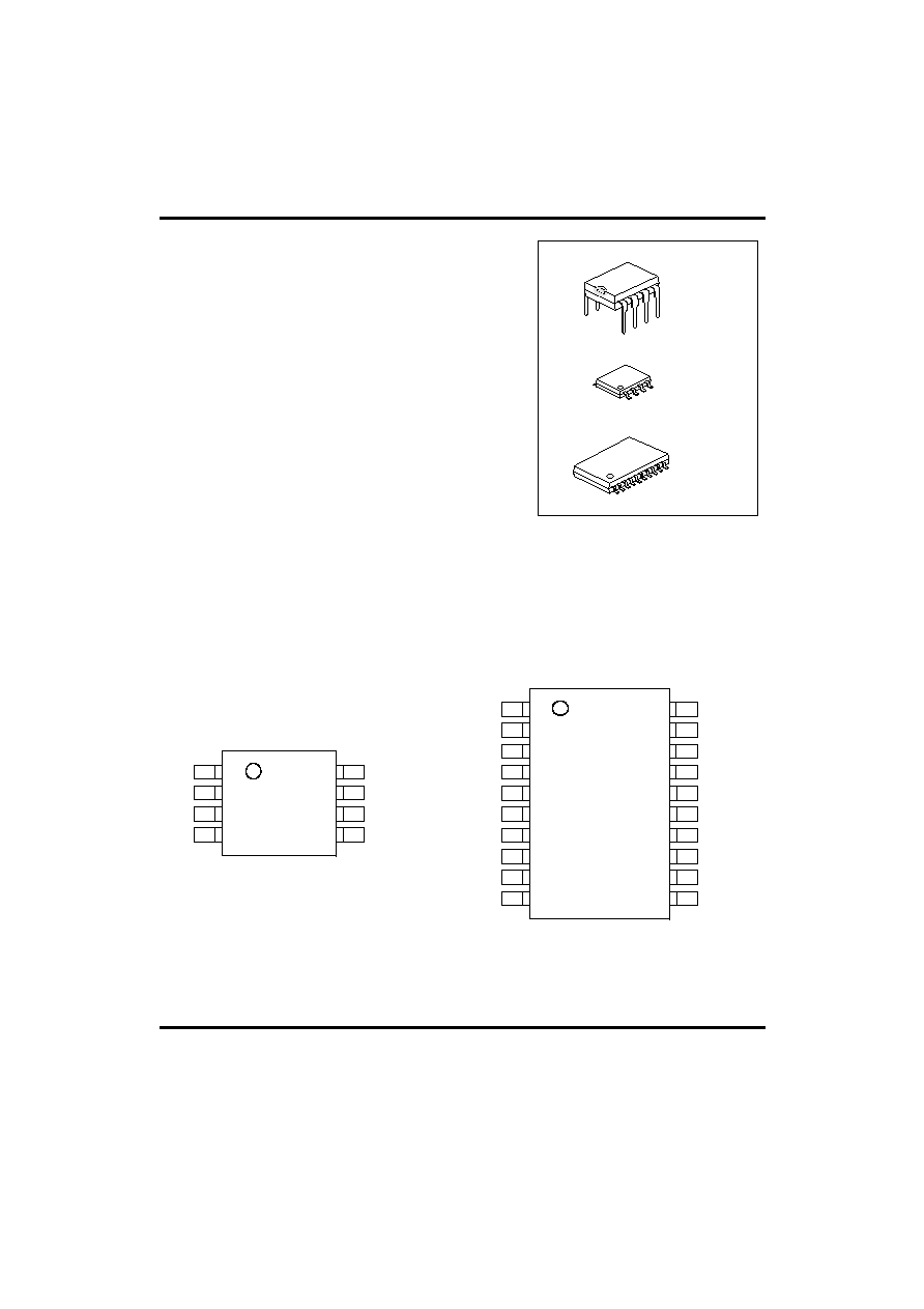
SOP-20
DIP-8
SOP-8
PIN CONNECTIONS
1
2
3
4
8
7
6
5
V
S
SI
Vz
CT
V
OUT
SO
RES
GND
DIP-8/SOP-8
1
2
3
4
8
7
6
5
V
S
SI
Vz
CT
V
OUT
SO
RES
GND
9
10
20
19
18
17
16
15
14
13
12
11
N.C.
GND
GND
GND
N.C.
N.C.
GND
GND
GND
GND
N.C.
N.C.
SOP-20
UTC L2949E
LINEAR INTEGRATED CIRCUIT
UTC
UNISONIC TECHNOLOGIES CO. LTD
2
QW-R102-014,A
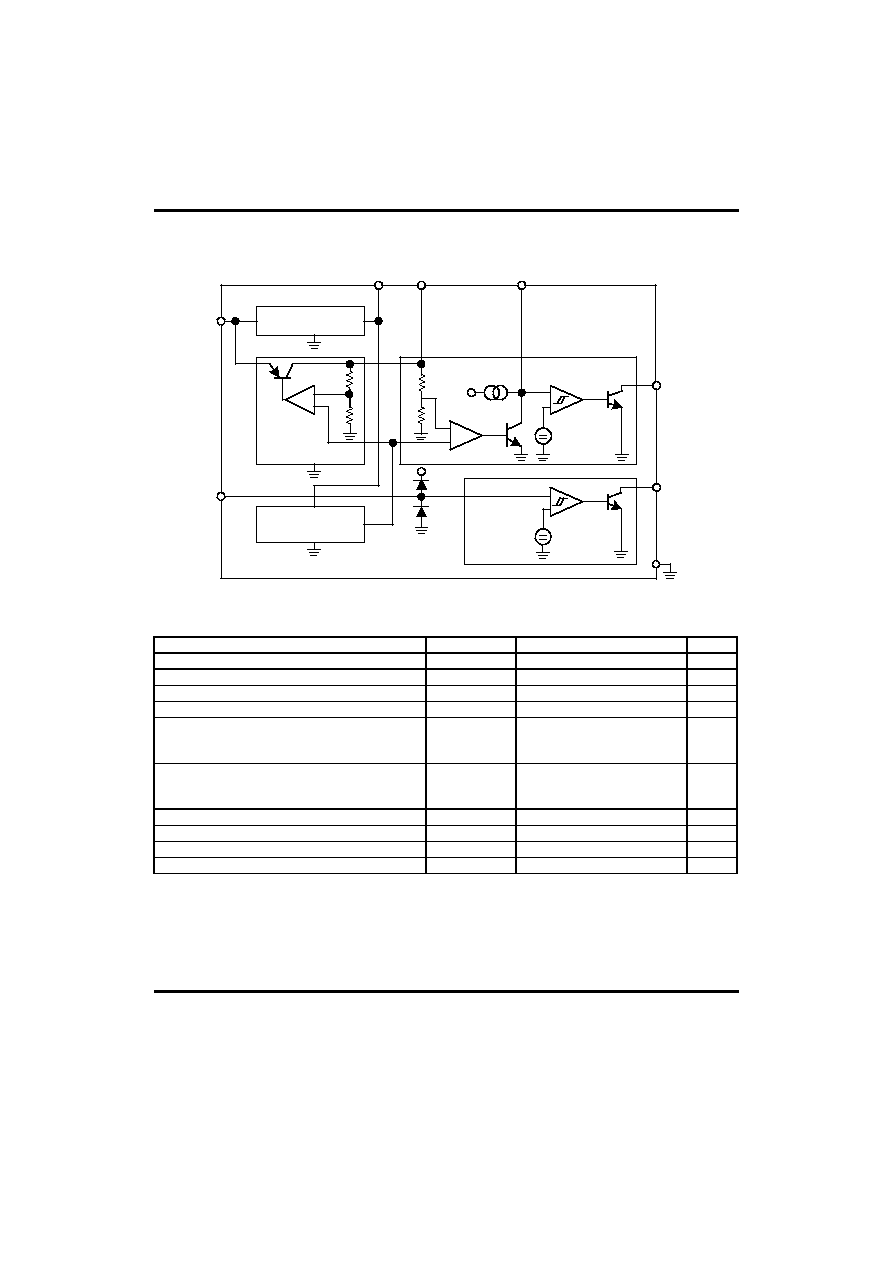
BLOCK DIAGRAM
Vz
V
OUT
CT
PREREGULATOR 5V
V
S
REG
SI
REF
1.23V
SENSE
1.23V
2V
RESET
2
+
V
S
GND
SO
RES
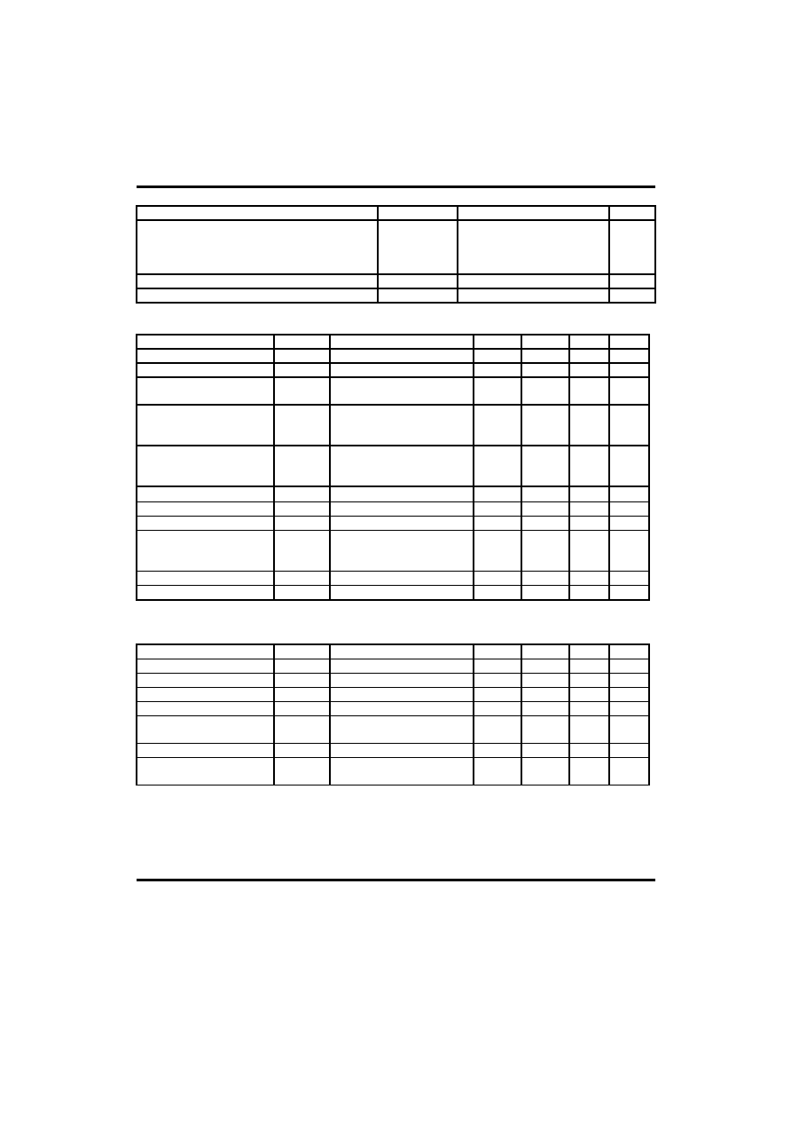
ABSOLUTE MAXIMUM RATINGS
PARAMETER SYMBOL
RATING
UNIT
DC Operating Supply Voltage
V
CC
28
V
Transient Supply Voltage(T<1s)
V
CC TR
40
V
Output Current
Io
Internally Limited
Output Voltage
Vo
20
V
Output Voltage
Reset Output
Sense Output
V
RES
Vso
20
20
V
Output Current
Reset Output
Sense Output
I
RES
Iso
5
5
mA
Preregulator Output Voltage
Vz
7
V
Preregulator Output Current
Iz
5
mA
Junction Temperature
Tj
-40+150
Storage Temperature Range
Tstg
-55+150
UTC L2949E
LINEAR INTEGRATED CIRCUIT
UTC
UNISONIC TECHNOLOGIES CO. LTD
3
QW-R102-014,A
THERMAL DATA
DESCRIPTION SYMBOL
RATING
UNIT
Thermal Resistance Junction-ambient
DIP-8
SOP-8
SOP-20
Rth j-amb
100
200
50
/W
Thermal Resistance Junction-pin (SOP-20)
Rth j-pins
15
/W
Thermal Shutdown Junction temperature
TJSD
165
ELECTRICAL CHARACTERISTICS
(Vs=14V;-40<Tj<125 unless otherwise specified)
PARAMETER SYMBOL CONDITIONS MIN
TYP.
MAX
UNIT
Output Voltage
Vo
Tj=25;Io=1mA
4.95 5 5.05
V
Output Voltage
Vo
6V<V
IN
<28V,1mA<Io<50mA 4.90 5 5.10 V
Output Voltage
Vo
V
IN
=40V;
T<1s 5mA<Io<100mA
4.75 5.25
V
Dropout voltage
V
D
Io=10mA
Io=50mA
Io=100mA
0.1
0.2
0.3
0.25
0.4
0.5
V
V
V
Input to Output Voltage
Difference in Undervoltage
Condition
V
IO
VIN=4V,Io=35mA
0.4
V
Max Output Leakage
Iouth ** V
IN
=25V,Vo=5.5V 20
50
80
A
Line Regulation
V
OL
6V<V
IN
<28V, Io=1mA
20
mV
Load Regulation
V
OLO
1mA<Io<100mA
30 mV
Current Limit
I
LIM
Vo=4.5V
Vo=4.5V,T
J
=25
Vo=0V(note 1)
105
120
200
100
400
400
mA
mA
Quiescent Current
I
QSE
Io=0.3mA;T
J
<100
200
300
A
Quiescent Current
I
Q
Io=100mA
5 mV
** With this test we guarantee that with no output current the output voltage will not exceed 5.5V
RESET
PARAMETER SYMBOL CONDITIONS MIN
TYP.
MAX
UNIT
Reset Thereshold Voltage
V
RT
Vo-0.5V
V
Reset Thereshold Hysteresis
V
RTH
50
100 200 mV
Reset Pulse Delay
t
RD
CT=100nF;TR100s
55 100
180
ms
Reset Output Low Voltage
V
RL
RRES=10K to Vs1.5V
0.4
V
Reset Output Gigh Leakage
Current
IRH VRES=5V
1 A
Delay Comparator Thereshold
V
CTth
2
V
Delay Comparator Thereshold
Hysteresis
V
CTth
,hy
100
mV
UTC L2949E
LINEAR INTEGRATED CIRCUIT
UTC
UNISONIC TECHNOLOGIES CO. LTD
4
QW-R102-014,A
SENSE
PARAMETER SYMBOL CONDITIONS MIN
TYP.
MAX
UNIT
Sense Low Thereshold
Vst
1.16
1.23
1.35
V
Sense Thereshold Hysteresis
Vsth
20
100
200
mV
Sense Output Low Voltage
V
SL
V
SI
1.16V;Vs3V
Rso=10K to Vo
0.4
V
Sense Output Leakage
I
SH
Vso=5V;V
SI
1.5V
1
A
Sense Input Current
I
SI
V
SI
=0 -20
-8
-3
A
PREREGULATOR
PARAMETER SYMBOL CONDITIONS MIN
TYP.
MAX
UNIT
Preregulator Output Voltage
Vz
Iz=10A
4.5 5 6 V
Preregulator Output Current
Iz
10
A
Note 1:Foldback characteristic
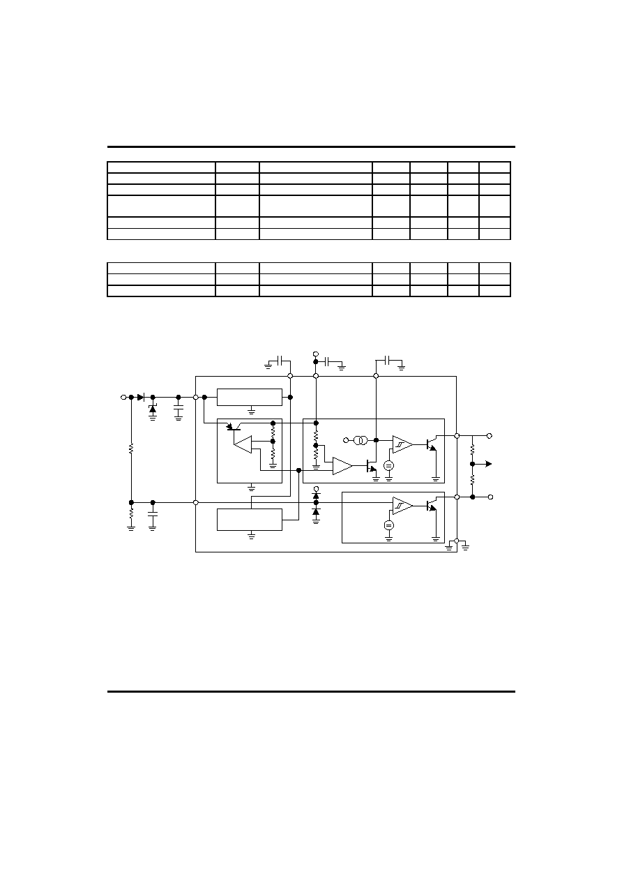
APPLICATION CIRCUIT
V
z
(optional)
V
OUT
CT
PREREGULATOR 5V
V
S
REG
SI
REF
1.23V
SENSE
1.23V
2V
RESET
2
+
V
S
GND
SO
RES
V
OUT
V
BAT
For stability:Cs1F, Co 4.7F, ESR<10at 10KHz
Recommended for application:Cs=Co=10µF to 100µF
APPLICATION INFORMATION
Suppl Voltage Transient
High supply voltage transients can cause a reset output signal disturbation.
For supply voltage greater than 8V the circuit shows a high immunity of the reset output against supply transients of
the reset output against supply transients of more than100V/s.
For supply voltages less than 8V supply transients of more than 0.4V/s can cause a reset signal disturbation.
To improve the transient behaviour for supply voltages less than 8V a capacitor at pin 3 can be used.
A capacitor at pin 3(C31F ) reduces also the output noise.
UTC L2949E
LINEAR INTEGRATED CIRCUIT
UTC
UNISONIC TECHNOLOGIES CO. LTD
5
QW-R102-014,A
FUNCTIONAL DESCRIPTION
The UTC L2949E is a monolithic integrated voltage regulator,based on the STM modular voltage regulator
approch.Several outstanding features and auxiliary functions are implemented to meet the requirements of supplying
microprocessor systems in automotive applications.Nevertheless,It is suitable also in other applications where the
present functions are required.The modular approach of this device allows to get easily also other features and
functions when required.
Voltage Regulator
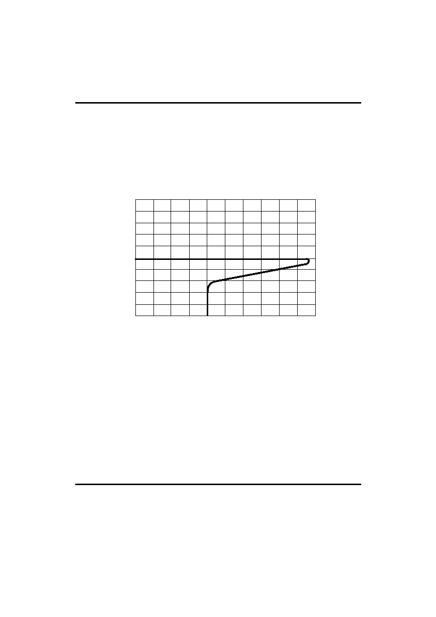
The voltage regulator uses an lsolated Collector Vertical PNP transistor as a regulating element.
5
0
20
100
200
I
OUT
(mA)
10
Figure 1: Foldback Characteristic of Vo
With this structure very low dropout voltage at currents up to 100mA is obtained.The dropout operation of the
standby regulator is maintained down to 3V input supply voltage.The output voltage is regulated up to the transient
input supply voltage of 4V.With this feature no functional interruption due to overvoltage pulses is generated.The
typical cuve showing the standby.output voltage as a function of the input supply voltage is shown in Fig.2. The
current consumption of the device(quiescent current) is less than 300A.
To reduce the quiescent current peak in the undervoltage region and to improve the transient response inthis
region.the dropout voltage is controlled,the quiescent current as a function of the supply input voltage is shown in
Fig.3.