 | –≠–ª–µ–∫—Ç—Ä–æ–Ω–Ω—ã–π –∫–æ–º–ø–æ–Ω–µ–Ω—Ç: Z90365 | –°–∫–∞—á–∞—Ç—å:  PDF PDF  ZIP ZIP |

CP97TEL2800
P R E L I M I N A R Y
1
1
P
RELIMINARY
C
USTOMER
P
ROCUREMENT
S
PECIFICATION
Z90365
1
D
IGITAL
T
ELEVISION
C
ONTROLLER
FEATURES
s
42-Pin SDIP
s
0
∞
C to +70
∞
C Temperature Range
s
Fully Customized Character Set
s
Character-Control and Closed-Caption Modes
s
Keypad User Control
s
TV Tuner Serial Interface
s
Direct Video Signals
s
Supports Violence Blocking
s
Speed: 12 MHz
GENERAL DESCRIPTION
The Z90365 Digital Television Controller is designed to
provide complete audio and video control of television re-
ceivers, video recorders, and advanced on-screen display
facilities. The television controller features a Z89C00 RISC
processor core that controls the on-board peripheral func-
tions and registers using the standard processor instruc-
tion set.
Character attributes can be controlled through two modes:
the on-screen display Character-Control Mode and the
Closed-Caption Mode. The Character-Control Mode pro-
vides access to the full set of attribute controls, allowing the
modification of attributes on a character-by-character ba-
sis. The insertion of control characters permits direction of
other character attributes. Closed-caption text can be de-
coded directly from the composite video signal and dis-
played on-screen with the assistance of the processor's
digital signal processing (DSP) capabilities.
The fully customized 512 character set, formatted in two
256 character banks, can be displayed with a host of dis-
play attributes that include underlining, italics, blinking,
eight foreground/background colors, character position off-
set delay, and background transparency.
Serial interfacing with the television tuner is provided
through the tuner serial port. Other serial devices, such as
digital channel tuning adjustments, may be accessed
through the industry-standard I
2
C port.
User control can be monitored through the keypad scan-
ning port, or the 16-bit remote control capture register. Re-
ceiver functions such as color and volume can be directly
controlled by eight 8-bit pulse width modulated ports.
Notes:
All Signals with a preceding front slash, "/", are
active Low. For example, B//W (WORD is active Low);
/B/W (BYTE is active Low, only).
Power connections follow conventional descriptions be-
low:
Device
ROM
(KW)
RAM*
(Words)
PWM
(8-Bit)
Voltage
Range
Z90365
32
640
8
4.5 to 5.5V
Note:
*General-Purpose
Connection
Circuit
Device
Power
V
CC
V
DD
Ground
GND
V
SS
Z90365
Digital Television Controller
Zilog
2
P R E L I M I N A R Y
CP97TEL2800
GENERAL DESCRIPTION
(Continued)
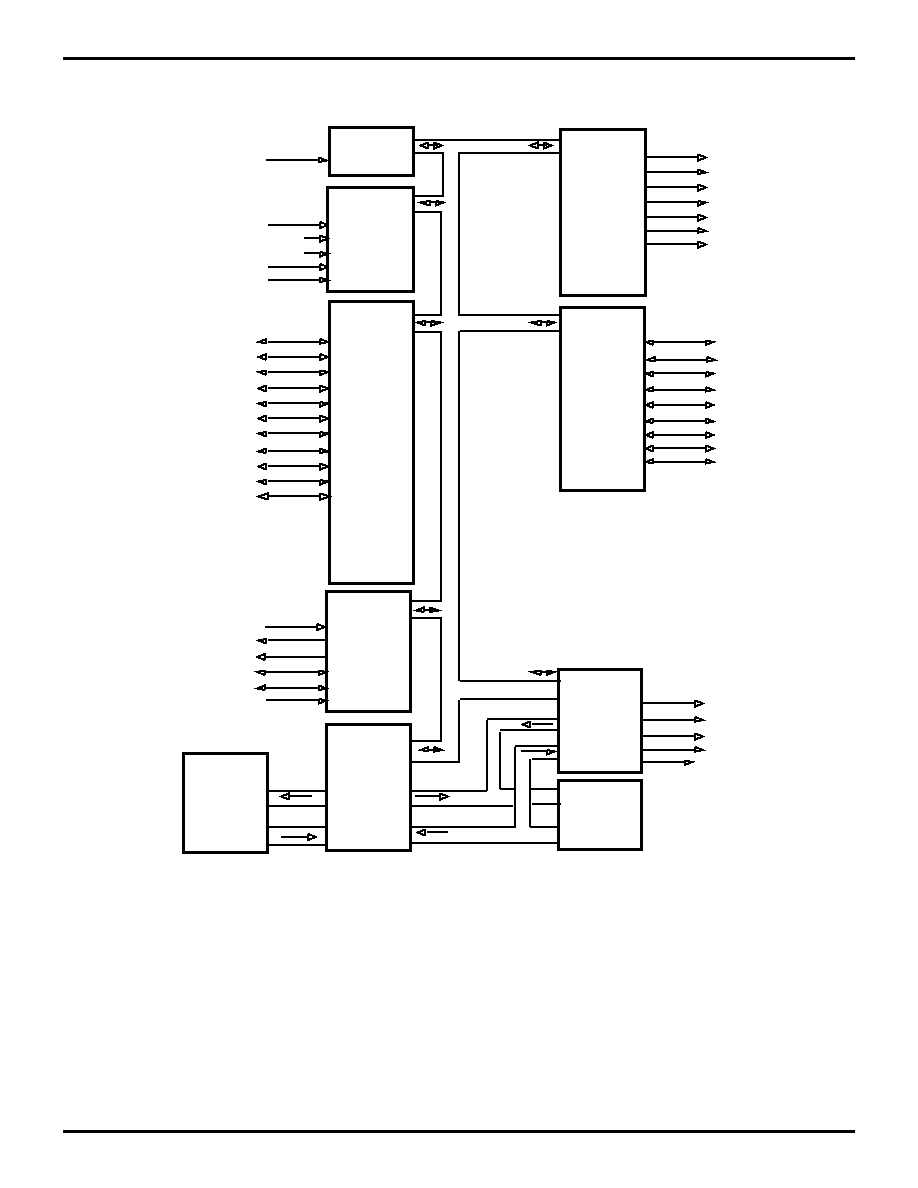
Figure 1. Functional Block Diagram
Capture
IRIN
ADC
ADC0
ADC1
ADC2
ADC3
ADC4
Port 0
Port 00
Port 01
Port 02
Port 03
Port 04
Port 05
Port 06
Port 07
Port 08
Port 09
Port 0F
Control
XTAL1
XTAL2
LPF
HSYNC
VSYNC
/Reset
CPU
RAM
640 x 16
ROM
32K x 16
OSD
V1
V2
V3
VBLANK
HALFBLNK
PWM
PWM1
PWM2
PWM3
PWM4
PWM5
PWM9
PWM10
Port1
Port 10
Port 11
Port 12
Port 13
Port 14
Port 15
Port 16
Port 17
Port 18
Port 17
Port 00
Register Addr/Data
Address
Data
ROM Data
ROM Addr
Port0F
Z90365
Zilog
Digital Television Controller
CP97TEL2800
P R E L I M I N A R Y
3
1
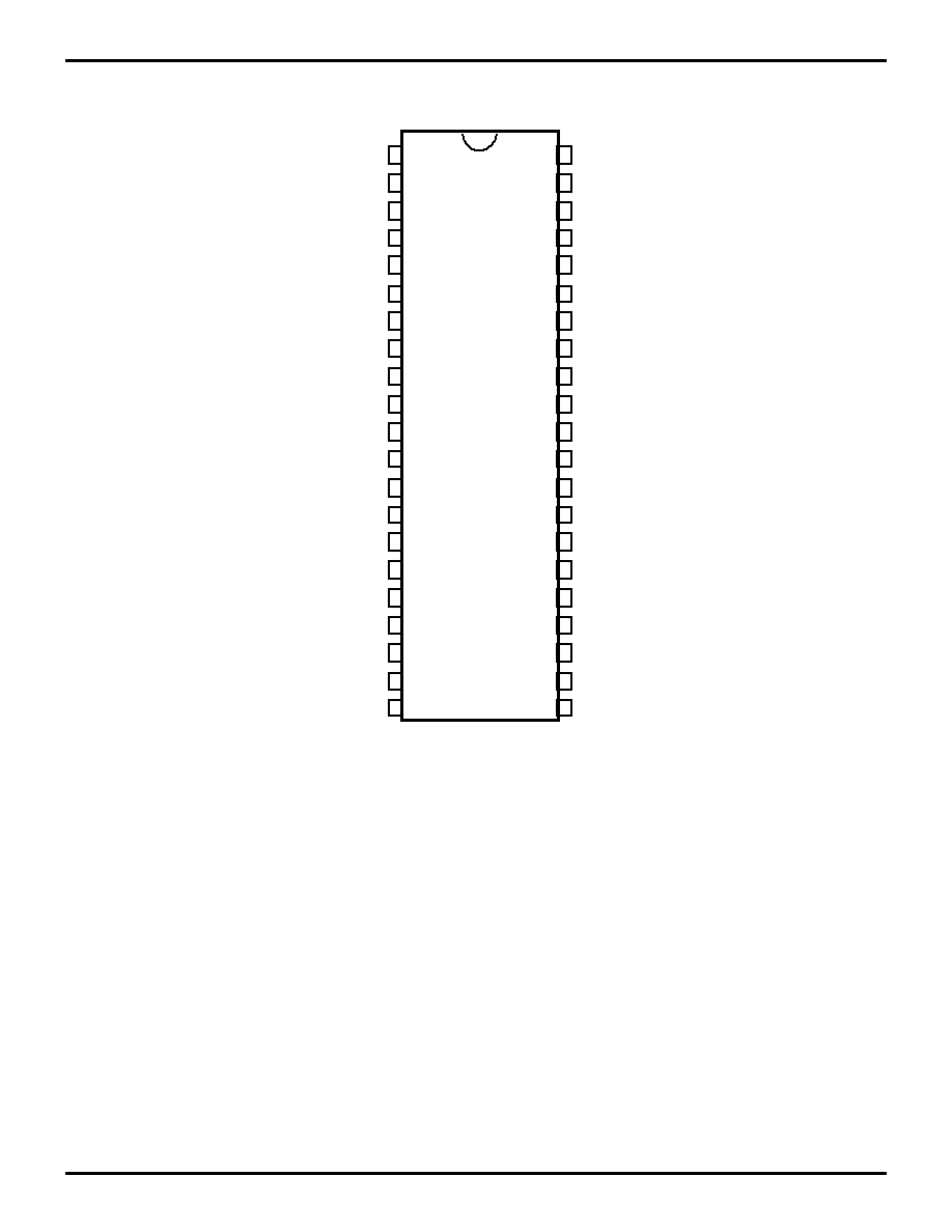
PIN DESCRIPTION
Figure 2. 42-Pin Shrink DIP
1
2
9
3
4
5
6
7
8
42
41
40
39
38
37
36
35
34
Port12/I2MSD
P11/I2MSC
Vcc
Port02/I2SSD
Port01/I2SSC
Port09
Port08/R<1>
IRIN
Port07/CSync
PWM10
PWM9
PWM4
PWM3
PWM2
PWM1
Port03
33
32
31
30
29
14
10
11
12
13
PWM5
Port00/ADC2
Port17/ADC1
GND
Port10/R<0>
/Reset
XTAL2
XTAL1
ANGND
LPF
15
28
27
26
25
24
23
20
16
17
18
19
Port04/ADC4
Port05/ADC3
Port06/Counter
Port18/G<0>
Port15/B<1>
Port16/SCLK
Port14/B<0>
Port13/G<1>
HSync
CVI/ADC0
VSync
VBlank
V1
V2
Z90365
Shrink
DIP
22
21
Port0F/Half Blank
V3

Z90365
Digital Television Controller
Zilog
4
P R E L I M I N A R Y
CP97TEL2800
PIN DESCRIPTION
(Continued)
Table 1. 42-Pin SDIP Pin Identification
Name
Function
Z90365
Direction
Reset
Notes
V
CC
+ 5 Volts
34
PWR
≠
GND
0 Volts
13, 30
PWR
≠
IRIN
Infrared Remote Capture
Input
36
I
I
ADC[4:0]
4-Bit A/D Converter Input
9, 10, 11, 12, 28
AI
I
PWM10, PWM9
14-Bit Pulse Width
Modulator Output
1, 2
O
O
PWM[5:1]
8-Bit Pulse Width Modulator
Output
3, 4, 5, 6, 7
O
O
Port0[F:0]
Bit Programmable
Input/Output Ports
21, -, -, -, -, -, 38, 37,
35, -, -, 15, 8, 40, 39,
11
B
I
1
Port1[8:0]
Bit Programmable
Input/Output Ports
16, 12, 20, 19, 18, 17,
42, 41, 14
B
I
SCL
I
2
C Clock I/O
39 or 41
BOD
2
SCD
I
2
C Data I/O
40 or 42
BOD
3
XTAL1
Crystal Oscillator Input
31
AI
I
XTAL2
Crystal Oscillator Output
32
AO
O
LPF
Loop Filter
29
AB
O
HSYNC
H_SYNC
26
B
I
VSYNC
V_SYNC
27
B
I
/Reset
Device Reset
33
I
I
V[3:1]
OSD Video Output Typically
Drive B, G, and R Outputs
22, 23, 24
O
O
Blank
OSD Blank Output
25
O
O
HalfBlank
OSD HalfBlank Output
21
O
4
RGB Digital
Outputs
R[1:0], G[1:0], and B[1:0]
Outputs of the RGB Matrix
37, 14, 17, 16, 19, 18
O
5
SCLK
Internal Processor SCLK
20
O
6
Notes:
1. SCL I/O pin is shared with Port 0 or Port 11.
2. SCD I/O pin is shared with Port 02 or Port 12.
3. Half Blank output is a function shared with Port 0F.
4. Digital RGB outputs and the internal SCLK are shared with Port 1 [5:0].
5. Internal processor SCLK is shared with Port 16.
PWM outputs are push/pull

Z90365
Zilog
Digital Television Controller
CP97TEL2800
P R E L I M I N A R Y
5
1
V1, V2, V3 (R, G, B) ANALOG OUTPUT (PRELIMINARY)
T
A
= 0
∞
C to 70
∞
C
Output Voltage (30 k
load)
Settling Time
V
CC
= 4.75
5.00V
5.25V
70% of DC level, 10pF load
data = 00
0.00v .. 0.65v
0.00v .. 0.70v
0.00v .. 0.75v
<
50 ns
data = 01
1.70v
±
0.20v
1.80v
±
0.20v
1.90v
±
0.20v
data = 10
2.80v
±
0.25v
2.90v
±
0.25v
3.00v
±
0.25v
data = 11
3.90v
±
0.3v
4.0v
±
0.30v
4.10v
±
0.30v
Figure 3. 32 kHz Oscillator Recommended Circuit
Figure 4. Recommended Low Pass Filter Circuit
Z90365
XTAL1
XTAL2
68 K
47 pF
22 pF
10 M
32.768 KHz
Z90365
47
µ
F
510
0.1
µ
F
Z90365
Digital Television Controller
Zilog
6
P R E L I M I N A R Y
CP97TEL2800
ABSOLUTE MAXIMUM RATINGS
DC CHARACTERISTICS
T
A
= 0
∞
C to + 70
∞
C; V
CC
= 4.5V to + 5.5V; F
OSC
= 32.768 kHz
Symbol
Parameter
Min
Max
Units
Conditions
V
CC
Power Supply Voltage
0
7
V
V
ID
Input Voltage
≠0.3
V
CC
+0.3
V
Digital Inputs
V
IA
Input Voltage
≠0.3
V
CC
+0.3
V
Analog Inputs (A/D0...A/D4)
V
O
Output Voltage
≠0.3
V
CC
+0.3
V
All Push-Pull Digital Output
V
O
Output Voltage
≠0.3
V
CC
+0.3
V
Push/Pull PWM Outputs (PWM1...PMW8)
I
OH
Output Current High
≠10
mA
One Pin
I
OH
Output Current High
≠100
mA
All Pins
I
OL
Output Current Low
20
mA
One Pin
I
OL
Output Current Low
200
mA
All Pins
T
A
Operating Temperature
0
70
∞
C
T
A
Storage Temperature
≠65
150
∞
C
Symbol
Parameter
Min
Max
Typical
Units
Conditions
V
IL
Input Voltage Low
0
0.2 V
CC
0.4
V
V
IH
Input Voltage High
0.7 V
CC
V
CC
3.6
V
V
PU
Max. Pull-Up Voltage
V
CC
+0.3
V
All Pins
V
OL
Output Voltage Low
0.4
0.16
V
@ I
OL
= 1 mA
V
OH
Output Voltage High
V
CC
≠0.4
4.75
V
@ I
OL
= 0.75 mA
V
XL
Input Voltage XTAL1 Low
0.3 V
CC
1.0
V
External Clock
V
XH
Input Voltage XTAL1 High
V
CC
≠2.0
3.5
V
Generator Driven
V
HY
Schmitt Hysteresis
3.0
0.75
0.5
V
On XTAL1 Input Pin
I
IR
Reset Input Current
150
90
µ
A
V
RL
= 0V
I
IL
Input Leakage
≠3.0
3.0
0.01
µ
A
@ 0V and V
CC
I
CC
Supply Current
100
60
mA
I
ADC
Input Current
10
µ
A
Notes:
1. The Z90365 should not be operated for extended periods with the crystal oscillator disconnected, except in the defined power-
down modes. In the event that the Z90365 is operated with the oscillator disconnected, the device may draw higher than typical
current.
2. Each line of the on-screen display can consist of any number of characters, up to a maximum of 30 characters.

Z90365
Zilog
Digital Television Controller
CP97TEL2800
P R E L I M I N A R Y
7
1
AC CHARACTERISTICS
T
A
= 0
∞
C to 70
∞
C; V
CC
= 4.5V to 5.25V; F
OSC
= 32.768 kHz
© 1997 by Zilog, Inc. All rights reserved. No part of this
document may be copied or reproduced in any form or by
any means without the prior written consent of Zilog, Inc.
The information in this document is subject to change
without notice. Devices sold by Zilog, Inc. are covered by
warranty and patent indemnification provisions appearing
in Zilog, Inc. Terms and Conditions of Sale only. Zilog, Inc.
makes no warranty, express, statutory, implied or by
description, regarding the information set forth herein or
regarding the freedom of the described devices from
intellectual property infringement. Zilog, Inc. makes no
warranty of merchantability or fitness for any purpose.
Zilog, Inc. shall not be responsible for any errors that may
appear in this document. Zilog, Inc. makes no commitment
to update or keep current the information contained in this
document.
Zilog's products are not authorized for use as critical
components in life support devices or systems unless a
specific written agreement pertaining to such intended use
is executed between the customer and Zilog prior to use.
Life support devices or systems are those which are
intended for surgical implantation into the body, or which
sustains life whose failure to perform, when properly used
in accordance with instructions for use provided in the
labeling, can be reasonably expected to result in
significant injury to the user.
Zilog, Inc. 210 East Hacienda Ave.
Campbell, CA 95008-6600
Telephone (408) 370-8000
FAX 408 370-8056
Internet: http://www.zilog.com
Symbol
Parameter
Min
Typical
Max
Units
T
PC
Input Clock Period
16
32
100
µ
S
T
RC
,T
FC
Clock Input Rise and Fall
12
nS
TD
POR
Power-On Reset Delay
0.8
1.2
S
TW
RES
Power-On Reset Minimum Width
5 TPC
µ
S
TD
HS
H-SYNC Incoming Signal Width
1
10
15
µ
S
TD
VS
V-SyYNC Incoming Signal Width
1
200
10,000
µ
S
TD
ES
Time Delay Between Leading Edge of V-SYNC and H-SYNC in
EVEN Field
≠12
0
+12
µ
S
TD
OS
Time Delay Between Leading Edge of H-SYNC in ODD Field
20
32
44
µ
S
TW
HVS
H_Sync/V_Sync Edge Width
0.5
2.0
µ
S
Note: All timing of the I
2
C bus interface are defined by related specifications of the I
2
C bus interface.

Z90365
Digital Television Controller
Zilog
8
P R E L I M I N A R Y
CP97TEL2800