 | –≠–ª–µ–∫—Ç—Ä–æ–Ω–Ω—ã–π –∫–æ–º–ø–æ–Ω–µ–Ω—Ç: ZM534 | –°–∫–∞—á–∞—Ç—å:  PDF PDF  ZIP ZIP |
Preliminary
ZM534
1
Quad 8 Bit DAC DIGITRIM
Features
À
2.7 - 5.5V Power Supply
À
Rail to Rail Input and Output
Voltage Range
À
Serial Three-Wire Interface
À
Software Shutdown
À
Simultaneous Update
À
Internal PON with Clear
À
Asynchronous Clear Input
À
Serial Data Output
À
16 Pin QSOP Package
À
Footprint Compatible to
MAXIM's MAX534/533
Applications
À
Digital Offset and Amplification
Adjustment
À
MPU controlled Trimming
Operations
À
Usage for General Voltage
Trimming Devices
General Description
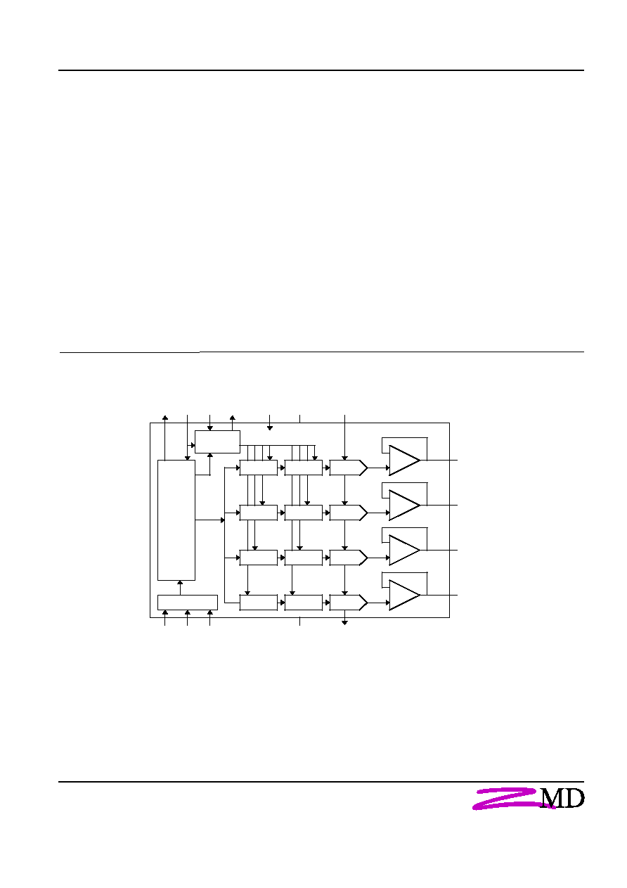
The DIGITRIM contains quad DAC
channels with identical structure.
There is an input register followed
by a DAC register, resistor string
DAC with externally supplied
reference and a rail-to-rail voltage
output buffer.
Using the three wire interface, data
is clocked serial into the 12 bit shift
register. Indepent from the four
adressing and command bits the
contents of shift register is
transfered to input register or DAC
register when /LDAC goes low ore
software command occures.
For daisy chaining applications
incoming data is outputed delayed
12 or 12 Ω SCLK - clocks at
DOUT.
After power on or hardware clear
all registers are set to zero.
The DIGITRIM circuits are
manufactured using a 0.8-micron
CMOS process.
Functional Diagram
/
CS
DIN
SCLK
OUTD
OUTC
OUTB
OUTA
DOUT
/CLR
/LDAC UPO
PDE
VDD
REFH
DGND
REFL
SR CTRL
DAC A
DAC B
DAC C
DAC D
DAC REG A
IN REG A
CONTRO
12 Bit
SHIFT
REG
ZM534
DAC REG B
IN REG B
DAC REG C
IN REG C
DAC REG D
IN REG D
Figure 1. Block Diagram

Preliminary
ZM534
2
Pin Configuration
ZMD
ZM534
OUTC
OUTD
REFL
V
DD
DGND
DIN
SCLK
/CS
OUTB
OUTA
REFH
UPO
PDE
/LDAC
/CLR
DOUT
Figure2. Pin Configuration
Pin Description
Name
Description
Name
Description
OUTB
DAC B Output
OUTC
DAC C Output
OUTA
DAC A Output
OUTD
DAC D Output
REFH
Reference Voltage Input (High)
REFL
Reference Voltage Input (Low)
UPO
User - Programmable Logic Output
VDD
Power Supply
PDE
Power Down Enable
GND
Ground
/LDAC
Load DAC register with the contents
of the input register
DIN
Serial Data Input
/CLR
Clear DAC Input
SCLK
Serial Clock Input
/DOUT
Serial Data Output
/CS
Chip-Select Input
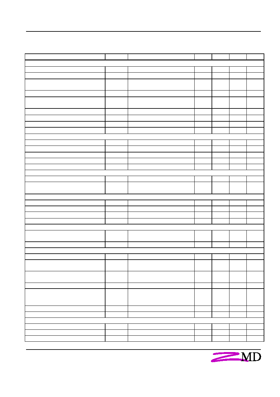
Operating Characteristics
Absolute Maximum Ratings
Stresses above those listed may cuuse permanent damage to the device. These are stress ratings only. Functional operation of this device
as indicated in this data sheet is not implied. Exposure to absolute maximum rating conditions for extended periods may effect device
reliability.
Parameter
Symbol
Min
Typ
Max
Unit
Power Supply voltage V
DD
to GND
V
DD
-0.3
+7
V
Digital Input Voltage to GND
V
I
-0.3
V
DD
+0.3
V
Digital Output Voltage to GND
-0.3
V
DD
+0.3
V
REFH/REFL Input Voltage
-0.3
V
DD
+0.3
V
OUTx Voltage
-0.3
V
DD
V
Maximum Current into Any Pin
50
mA
Continuous Power Dissipation
(TA= + 70
o
C) QSOP16
P
500
mW
Operating Temperature Range
T
-45
+85
o
C
Storage Temperature Range
T
stg
-55
+125
o
C
Preliminary
ZM534
3
Electrical Characteristics
(V
DD
=+2,7 to +5.5V, V
REFH
=4V, REFL=GND=0V, R
L
=10k
, C
L
=100pF,T
A
=T
MIN
to T
MAX
, Typical values are at V
DD
= +5V and T
A
= +25
o
C)
Parameter
Symbol
Conditions
Min
Typ
Max
Unit
Static Accuracy
Resolution
8
Bits
Integral Nonlinearity
INL
(Note1)
±
1
LSB
Differential Nonlinearity
DNL
Garanteed monotonic (all
codes) (Note 1)
±
1
LSB
Zero-Code Error
Code=00 hex
±
20
mV
Zero-Code-Error Supply Rejection
Code=00 hex, VDD=4.5 to
5.5V
1
LSB
Zero Code Temperatur Coefficient
Code=00 hex
±
10
µV/
O
C
Full Scale Error
Code=FF hex
±
20
mV
Full-Scale Error Supply Rejection
Code=FF hex
1
LSB
Full-Scale Temperature Coefficient
Code=FF hex
±
10
µV/
O
C
Reference Inputs
Input Voltage Range
0
V
DD
V
Input Resistance
85
k
Input Capacitance
10
pF
Channel-to-Channel Isolation
(Note 2)
-60
dB
AC Feedthrough
(Note 3)
-60
dB
DAC Outputs
Output Voltage Range
R
L
=open
0
V
REFH
V
Load Regulation
Code=FF hex, RL from 10k
to oo
0.25
LSB/m
A
Digital Inputs
Input High Voltage
V
IH
0.7V
DD
V
Input Low Voltage
V
IL
0.3V
DD
V
Input Current
I
IN
VIN=0V or V
DD
±
1.0
µA
Input Cpacitance
C
IN
(Note 4)
10
pF
Digital Outputs
Output High Voltage
V
OH
I
SOURCE
=0.1mA
V
DD
-
0.5
V
Output Low Voltage
V
OL
I
SINK
=2mA
0.4
V
Dynamic Performence
Voltage-Output Slew Rate
Code=FF hex
0.8
V/µs
Output Settling Time
To Ω LSB, from code 00 to
code FF hex (Note 5)
7
µs
Digital Feedthrough and Crosstalk
V
REFH
=0V, code 00 to FF hex
(Note 6)
4
nV-s
Digital-to Analog Glitch Impulse
Code 80 hex to code 7F hex
45
nV-s
Signal-to-Noise Plus Distorsion Ratio SINAD
V
REFH
=4V
p-p
, at 1kHz, code=FF
hex/
V
REFH
=4V
p-p
, at 10kHz
80/70
dB
Multiplying Bandwidth
V
REFH
=0.5V
p-p
, 3dB bandwitdh
500
kHz
Wideband Amplifier Noise
60
µV
RMS
Power Supplies
Power-Supply Voltage
V
DD
2,7
5.5
V
Supply Current
I
DD
1,3
mA
Shutdown Current
2.5
10
µA
Preliminary
ZM534
4
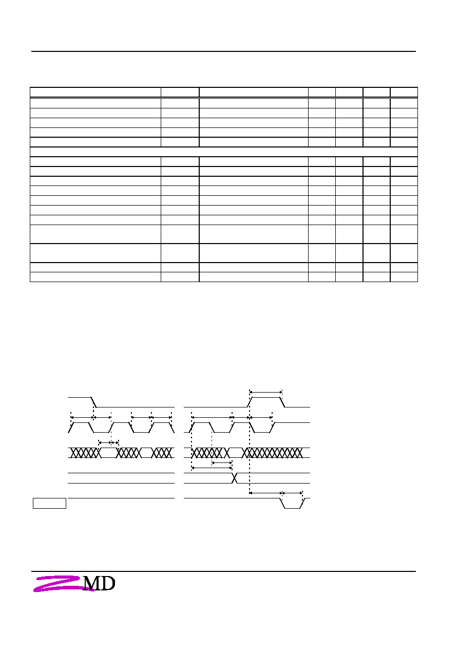
Timing Characteristics
(V
DD
=+4.5 to +5.5V, V
REFH
=4V, REFL=GND=0V, C
L
=100pF,T
A
=T
MIN
to T
MAX
, Typical values are at V
DD
= +5V and TA= +25
o
C)
Parameter
Symbol
Conditions
Min
Typ
Max
Unit
V
DD
Rise to/CS Fall Setup Time
t
DSC
50
µs
/LDAC Pulse Widt Low
t
LDAC
40
20
ns
/CS Rise to /LDAC Fall Setup Time
t
CLL
40
ns
/CLR Pulse Witdh Low
t
CLW
40
20
ns
/CS Pulse Width High
t
CSW
90
ns
Serial Interface Timing
SCLK Clock Frequency (Note 8)
f
CLK
10
MHz
SCLK Pulse Width High
t
CH
40
ns
SCLK Pulse Width Low
t
CL
40
ns
/CS Fall to SCLK Rise Setup Time
t
CSS
40
ns
SCLK Rise to /CS Rise Hold Time
t
CSH
0
ns
DIN to SCLK Rise to Setup Time
t
DS
40
ns
DIN to SCLK Rise to Hold Time
t
DH
0
ns
SCLK Rise to DOUT Valid
propagation Delay Time (Note 9)
t
DO1
200
ns
SCLK Fall to DOUT Valid
propagation Delay Time (Note 10)
t
DO2
210
ns
SCLK Rise to /CS Fall Delay
t
CS0
40
ns
/CS Rise to SCLK Rise Setup Time
t
CS1
40
ns
Note 1:
INL and DNL are measured with R
L
referenced to Ground. Nonlinearity is measured from the first code that is greater than or
equal to the maximum offset specification to the code FF hex (full scale).
Note 2:
V
REFH
= 4Vp-p, 10kHz. Channel to-channel isolation is measured by setting one DAC's code to FF hex and setting all other DAC's
codes to 00H.
Note 3:
V
REFH
=4Vp-p, 10kHz. DAC code = 00 hex.
Note 4:
Gurantedby design not production tested.
Note 5:
Output settling time is measured from 50% point of the rising edge of /CS to Ω LSB of VOUT's final value.
Note 6:
Digital crosstalk is defined as the glitch energy at any DAC output in response to a full-scale step change on any other. DAC
Note 7:
If /LDAC is activated prior to /CS rising edge, it must stay low for t
LDAC
or longer after /CS goes high.
Note 8:
When DOUT is not used. If DOUT is used, f
SCLK
max is 4 MHz, due to DOUT propagation delay.
Note 9:
Serial data clocked out at SCLK's rising edge (measured from 50% of the clock edge to 20% or 80% of V
DD
Note10: Serial data clocked out at SCLK's falling edge (measured from 50% of the clock edge to 20% or 80% of V
DD
/CS
SCLK
DIN
DOUT
/LDAC
t
CSO
t
CSS
t
CL
t
CH
t
DS
t
DH
t
CSW
t
CP
t
CSH
t
CS1
t
CLL
t
LDAC
t
D01
t
D02
Figure 3. Serial-Interface Timing Diagram

Preliminary
ZM534
5
Programming the DIGITRIM
To program the DIGITRIM a serial bit stream is
provided to input DIN.
The DIN data bits are clocked in a 12 Bit shift
register with rising edge of SCLK. while /CS=Low
That means, only the last 12 Bits are important.
Data can be transfered in blocks. Between the
blocks SCLK should remaining on low level.
With the raising edge of /CS data will be clocked
into input register and commands will be executed.
Serial Data Format
first bits last bits
A1
A0
C1
C0
D7 D6 D5 D4 D3 D2 D1 D0
Adress and Control Bits
Data Bits
Serial-Interface Programming Commands
A1
A0 C1 C0 D7..D0
/LDAC
Function
Load Input Register
0
0
0
1
8-bit DAC data
1
Load Input Register A, outputs unchanged
0
1
0
1
8-bit DAC data
1
Load Input Register B, outputs unchanged
1
0
0
1
8-bit DAC data
1
Load Input Register C, outputs unchanged
1
1
0
1
8-bit DAC data
1
Load Input Register D, outputs unchanged
Load Input Register and update all DAC-Registers on /CS rising edge
0
0
1
1
8-bit DAC data
1
Load Input Register A, outputs updated
0
1
1
1
8-bit DAC data
1
Load Input Register B, outputs updated
1
0
1
1
8-bit DAC data
1
Load Input Register C, outputs updated
1
1
1
1
8-bit DAC data
1
Load Input Register D, outputs updated
Software /LDAC, update all DAC registers with input register data on /CS rising edge, leave shutdown
0
1
0
0
XXXXXXXX
1
Update all DAC registers with input register data
Load all DAC register with the shift register data
1
0
0
0
8-bit DAC data
X
Update all DAC outputs with the serial data
Software Shutdown for all buffer amplifier, contents of register remains
1
1
0
0
XXXXXXXX
X
Reduces power consumtion rapidely
User-Programmable Output programming
0
0
1
0
XXXXXXXX
X
UPO goes LOW
0
1
1
0
XXXXXXXX
X
UPO goes High
No operation
0
0
0
0
XXXXXXXX
X
Allows to shift data througt IC without effect in daisy chaining
applications
SET DOUT Phase, update all DAC registers
1
1
1
0
XXXXXXXX
X
DOUT data valid at SCLK rising, Mode 1)
1
0
1
0
XXXXXXXX
X
DOUT data valid at SCLK falling, Mode 0 default)